


ņä£ļĪĀ
ņĄ£ĻĘ╝ ĒÖöņäØ ņŚ░ļŻīņØś Ļ│ĀĻ░ł ļ░Å ĻĖ░Ēøä ļ│ĆĒÖö ļ¼ĖņĀ£ļź╝ ĒĢ┤Ļ▓░ĒĢĀ ļ░®ļ▓Ģņ£╝ļĪ£ ņ╣£ĒÖśĻ▓Į ņŗĀņ×¼ņāØ ņŚÉļäłņ¦ĆņŚÉ ļīĆĒĢ£ ņŚ░ĻĄ¼Ļ░Ć ĻĖēņ”ØĒĢśĻ│Ā ņ׳ļŗż. ņŚ¼ļ¤¼ Ļ░Ćņ¦Ć ņŗĀņ×¼ņāØ ņŚÉļäłņ¦Ć ņ×ÉņøÉ ņżæ, Ēā£ņ¢æ ņŚÉļäłņ¦Ćļź╝ ņĀäĻĖ░ ļ░Å ĒÖöĒĢÖņĀü ņŚÉļäłņ¦ĆļĪ£ ņĀäĒÖśĒĢśņŚ¼ ņé¼ņÜ®ĒĢśļŖö ļ░®ļ▓ĢņØ┤ ĒśäņŗżņĀüņØĖ ļīĆņĢł ņżæ ĒĢśļéśļĪ£ ĻĖ░ļīĆļÉśĻ│Ā ņ׳ļŗż. ĒĢśņ¦Ćļ¦ī Ēā£ņ¢æ ņŚÉļäłņ¦Ć ļ│ĆĒÖś ņŗ£ņŖżĒģ£ņØś ļ╣äņÜ®ņØ┤ ĻĖ░ņĪ┤ ĒÖöņäØ ņŚ░ļŻī ĻĖ░ļ░ś ņŚÉļäłņ¦Ć ņŗ£ņŖżĒģ£ņŚÉ ļ╣äĒĢ┤ Ļ│ĀĻ░ĆņØ┤ļ»ĆļĪ£, Ēā£ņ¢æ ņŚÉļäłņ¦Ć ļ│ĆĒÖś ņŗ£ņŖżĒģ£ņØś ņäżņ╣ś ļ░Å ļ░£ņĀäņŚÉ ņ¢┤ļĀżņøĆņØä Ļ▓¬Ļ│Ā ņ׳ļŗż.
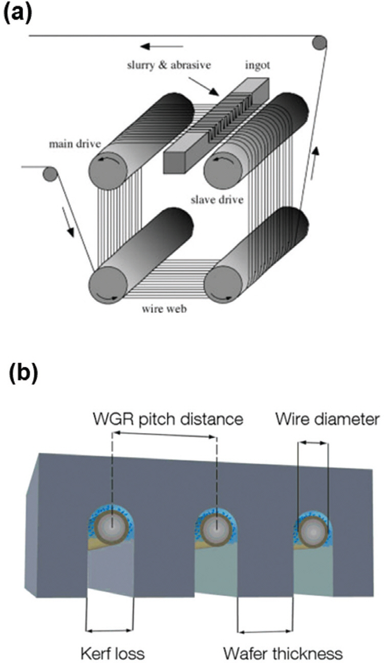
Ēā£ņ¢æ ņŚÉļäłņ¦Ćļź╝ ņĀäĻĖ░ļĪ£ ņĀäĒÖśĒĢśļŖö Ēā£ņ¢æĻ┤æ ļ¬©ļōł ņŗ£ņŖżĒģ£ņØś Ļ▓ĮņÜ░ ņĀ£ņ×æ ļ╣äņÜ® ņżæ ņĢĮ 40%Ļ░Ć Ļ┤æĒØĪņłśņĖĄņ£╝ļĪ£ ņé¼ņÜ®ĒĢśļŖö ņŗżļ”¼ņĮś ĻĖ░ĒīÉņØ┤ ņ░©ņ¦ĆĒĢ£ļŗż.1) ļö░ļØ╝ņä£, Ēā£ņ¢æĻ┤æ ļ¬©ļōł ņŗ£ņŖżĒģ£ņØś ļ╣äņÜ® Ļ░Éņåīļź╝ ņ£äĒĢ┤ņä£ļŖö ņŗżļ”¼ņĮś ĻĖ░ĒīÉ Ļ░ĆĻ▓® Ļ░ÉņåīĻ░Ć ņŻ╝ņÜöĒĢśļŗżĻ│Ā ļ│╝ ņłś ņ׳ļŗż. ņŗżļ”¼ņĮś ĻĖ░ĒīÉņØ┤ Ļ░ĆĻ▓®ņØ┤ ļåÆņØĆ ņØ┤ņ£ĀļŖö, Ļ▓░ņĀĢņ¦ł ņŗżļ”¼ņĮś ņ×ēĻ││ņŚÉņä£ ņø©ņØ┤ĒŹ╝ (wafer) ĒśĢĒā£ļĪ£ ņ×Éļź┤ļŖö ņø©ņØ┤ĒŹ╝ļ¦ü Ļ│ĄņĀĢ ĻĖ░ņłĀņŚÉņä£ ļ░£ņāØĒĢśļŖö ņ×¼ļŻī ņåÉņŗż ļ░Å ņČ®ļČäĒ׳ ņ¢ćņØĆ ļæÉĻ╗śņØś ņø©ņØ┤ĒŹ╝ ņĀ£ņ×æņØ┤ ņ¢┤ļĀĄĻĖ░ ļĢīļ¼ĖņØ┤ļŗż. Fig. 1 ņØĆ Ēśäņ×¼ Ēā£ņ¢æĻ┤æ ņé░ņŚģņŚÉņä£ ņé¼ņÜ®ĒĢśĻ│Ā ņ׳ļŖö ņŗżļ”¼ņĮś ņø©ņØ┤ĒŹ╝ļ¦ü ĻĖ░ņłĀņØĖ ļŗżņżæ ņÖĆņØ┤ņ¢┤ ņÅśņ×ē (multi-wire sawing) ĻĖ░ņłĀņØä ļ│┤ņŚ¼ ņŻ╝Ļ│Ā ņ׳ļŗż. ļŗżņżæ ņÖĆņØ┤ņ¢┤ ņÅśņ×ē ĻĖ░ņłĀņØĆ ņøÉĒåĄ ļ¬©ņ¢æņØś Ļ▓░ņĀĢņ¦ł ņŗżļ”¼ņĮś ņ×ēĻ││ņØä ņø©ņØ┤ĒŹ╝ ĒśĢĒā£ļĪ£ ļ¦īļōżĻĖ░ ņ£äĒĢ┤ņä£, ņ¦äļÅÖĒĢśļŖö ļŗżņżæ ņÖĆņØ┤ņ¢┤Ļ░Ć ņŗżļ”¼ņĮś ņ×ēĻ││ņØä ņĀłņéŁ ĒĢśļ®┤ņä£ ĒåĄĻ│╝ĒĢśĻ▓ī ļÉ£ļŗż. ņØ┤ļĢī, ņÖĆņØ┤ņ¢┤ ļæÉĻ╗śļ¦īĒü╝ņØś ņ×¼ļŻī ņåÉņŗżņØ┤ ļ░£ņāØĒĢśļ®░ ņØ┤ļź╝ kerf-lossļØ╝Ļ│Ā ĒĢ£ļŗż. Kerf-lossļŖö 180 ╬╝m ļæÉĻ╗śņØś ņŗżļ”¼ņĮś ņø©ņØ┤ĒŹ╝ļź╝ ņĀ£ņ×æ ĒĢĀ ļĢī ļīĆļץ 40% Ļ░Ć ļ░£ņāØĒĢ£ļŗż. ļŗżņżæ ņÖĆņØ┤ņ¢┤ ņÅśņ×ē ĻĖ░ņłĀņØś ļśÉ ļŗżļźĖ ĒĢ£Ļ│äņĀÉņØĆ 100 ╬╝m ņØ┤ĒĢś ļæÉĻ╗śņØś ņŗżļ”¼ņĮś ņø©ņØ┤ĒŹ╝ļź╝ ņĀ£ņ×æĒĢśĻĖ░ ņ¢┤ļĀżņÜ░ļ®░, ņØ┤ļ│┤ļŗż ņ¢ćņØĆ ļæÉĻ╗śņØś ņŗżļ”¼ņĮś ņø©ņØ┤ĒŹ╝ ņĀ£ņĪ░ ņŗ£, ņłśņ£©ņØ┤ ĻĖēĻ▓®Ē׳ Ļ░ÉņåīĒĢśļŖö ļ¼ĖņĀ£Ļ░Ć ļ░£ņāØĒĢ£ļŗż.
ņĄ£ĻĘ╝ņŚÉļŖö ĻĖ░ņĪ┤ņØś ļŗżņżæ ņÖĆņØ┤ņ¢┤ ņÅśņ×ē ĻĖ░ļ░śņØś ņø©ņØ┤ĒŹ╝ļ¦ü ĻĖ░ņłĀņØś ļŗ©ņĀÉņØä ĒĢ┤Ļ▓░ĒĢśļ®┤ņä£, ņĄ£ņóģņĀüņ£╝ļĪ£ļŖö 50 ╬╝m ļæÉĻ╗ś ņØ┤ĒĢśņØś ņŗżļ”¼ņĮś ņø©ņØ┤ĒŹ╝ļź╝ kerf-loss ņŚåņØ┤ ņĀ£ņ×æĒĢśļŖö ņĀĆ ļ╣äņÜ®ņØś ņŗżļ”¼ņĮś ĻĖ░ĒīÉ ņāØņé░ ĻĖ░ņłĀņŚÉ ļīĆĒĢ£ ņŚ░ĻĄ¼Ļ░Ć Ļ┤æļ▓öņ£äĒĢśĻ▓ī ņ¦äĒ¢ēļÉśņŚłļŗż. ņØ┤ļ¤¼ĒĢ£ ņŚ░ĻĄ¼ ņżæņŚÉ ĒĢśļéśļĪ£, ņØśļÅäņĀüņ£╝ļĪ£ ļ░śļÅäņ▓┤ ĻĖ░ĒīÉņŚÉ ĻĘĀņŚ┤ ļ░£ņāØ ļ░Å ņ¦äņĀäņØä ĒåĄĒĢ┤ ļ░śļÅäņ▓┤ ļ░Ģļ¦ēņØä ļ░Ģļ”¼ņŗ£ĒéżļŖö ĻĘĀņŚ┤ ĻĖ░ļ░ś ļ░Ģļ”¼ ĻĖ░ņłĀņØ┤ Ļ░£ļ░£ļÉśņŚłļŗż. ņØ┤ļ¤¼ĒĢ£ ĻĘĀņŚ┤ ĻĖ░ļ░ś ļ░Ģļ”¼ ĻĖ░ņłĀņØĆ, ĻĖ░ņĪ┤ ņø©ņØ┤ĒŹ╝ļ¦ü ĻĖ░ņłĀņØś ĒĢ£Ļ│äņĀÉņØĖ kerf-lossĻ░Ć ļ░£ņāØĒĢśņ¦Ć ņĢŖņ£╝ļ®░, 100 ╬╝m ņØ┤ĒĢś ļæÉĻ╗śļź╝ Ļ░Ćņ¦ĆļŖö Ļ▓░ņĀĢņ¦ł ļ░śļÅäņ▓┤ ņø©ņØ┤ĒŹ╝ļź╝ ņåÉņēĮĻ▓ī ņĀ£ņ×æ Ļ░ĆļŖźĒĢśļŗż. ļ┐Éļ¦ī ņĢäļŗłļØ╝, ĻĘĀņŚ┤ ĻĖ░ļ░ś ļ░Ģļ”¼ ĻĖ░ņłĀļĪ£ ņĀ£ņ×æļÉśļŖö ļ░śļÅäņ▓┤ ĻĖ░ĒīÉņØä ĻĖ░ļ░śņ£╝ļĪ£ ĒĢ£ Ēā£ņ¢æ ņŚÉļäłņ¦Ć ļ│ĆĒÖś ņåīņ×ÉļŖö ņ£ĀņŚ░ĒĢśļ®┤ņä£ Ļ░Ćļ▓╝ņÜ┤ ĒŖ╣ņä▒ņØ┤ ņ׳ņ¢┤ ĻĖ░ņĪ┤ņØś ļæÉĻ║╝ņÜ┤ Ēā£ņ¢æ ņŚÉļäłņ¦Ć ņĀäĒÖś ņåīņ×Éļ│┤ļŗż ĒÖ£ņÜ®ļÅäĻ░Ć ļ¦żņÜ░ ļåÆļŗżĻ│Ā ĒĢĀ ņłś ņ׳Ļ▓Āļŗż. ļ│Ė ļģ╝ļ¼ĖņŚÉņä£ļŖö, Ēśäņ×¼ Ļ░£ļ░£ļÉśĻ│Ā ņ׳ļŖö ĻĘĀņŚ┤ ĻĖ░ļ░ś ļ░Ģļ”¼ ĻĖ░ņłĀ ļ░Å ņØ┤ļź╝ ņØ┤ņÜ®ĒĢ£ ņĀĆļ╣äņÜ® Ēā£ņ¢æ ņŚÉļäłņ¦Ć ļ│ĆĒÖś ņåīņ×É Ļ░£ļ░£ ļÅÖĒ¢źņØä ņé┤ĒÄ┤ļ│┤Ļ│Āņ×É ĒĢ£ļŗż.
ĻĘĀņŚ┤ ĻĖ░ļ░ś ļ░Ģļ¦ē ļČäļ”¼ ĻĖ░ņłĀ
2-1 ĻĘĀņŚ┤ ĻĖ░ļ░ś ļ░Ģļ¦ē ļČäļ”¼ ĻĖ░ņłĀ ņøÉļ”¼
ņ×¼ļŻīņØś ĻĘĀņŚ┤ņØĆ ņØĖņĀæĒĢ£ ņøÉņ×É Ļ░äņØś Ļ▓░ĒĢ®ņØ┤ ļ¼╝ļ”¼ņĀüņØĖ Ēīī Ļ┤┤ļĪ£ ņØĖĒĢ┤ ļüŖņ¢┤ņ¦Ćļ®┤ņä£ ņāłļĪ£ņÜ┤ Ēæ£ļ®┤ņØ┤ ĒśĢņä▒ļÉśļŖö ĒśäņāüņØä ļ¦ÉĒĢ£ļŗż. ĻĘĀņŚ┤ņØ┤ ļ░£ņāØĒĢśĻĖ░ ņ£äĒĢ┤ņä£ļŖö ĻĖ░Ļ│äņĀü ĒלņŚÉ ņØśĒĢ┤ ņ£ĀļÅäļÉ£ energy release rate GĻ░Ć ņ×¼ļŻīņØś ĻĘĀņŚ┤ ļ░£ņāØņØä ņĀĆĒĢŁĒĢśļŖö ļŖźļĀźņØĖ toughness G cĻ░ÆņØä ņ┤łĻ│╝ĒĢĀ ļĢī ļ░£ņāØĒĢ£ļŗż.4) ļ░śļÅäņ▓┤ ĻĖ░ĒīÉ ņ£äņŚÉ ļ░Ģļ¦ēņØ┤ ĒśĢņä▒ļÉśņ¢┤ ņ׳ļŖö Ļ▓ĮņÜ░, ļ░Ģļ¦ēņŚÉņä£ ļ░£ņāØĒĢ£ ņ×öļźś ņØæļĀźņ£╝ļĪ£ ņØĖĒĢ┤ ĻĘĀņŚ┤ ļ░£ņāØ ņĪ░Ļ▒┤ (G > G c) ņØ┤ ņČ®ņĪ▒ļÉśļ®┤ ĻĘĖļ”╝2ņÖĆ Ļ░ÖņØ┤ surface crack, channeling, substrate damage, spalling, debonding ļō▒ ļŗżņ¢æĒĢ£ ĻĘĀņŚ┤ Ēī©Ēä┤ņØ┤ ļ░£ņāØĒĢ£ļŗż.5ŌĆō7) ņØ┤ļĢī, ļ░śļÅäņ▓┤ ĻĖ░ĒīÉĻ│╝ ļ░Ģļ¦ēņØś ņŚ░ņä▒, ņ×öļźś ņØæļĀź ļ░®Ē¢ź ļ░Å ļ░śļÅäņ▓┤ ĻĖ░ĒīÉĻ│╝ ļ░Ģļ¦ēņØś Ļ│äļ®┤ Ļ▓░ĒĢ® ņāüĒā£ņŚÉ ļö░ļØ╝ Ļ░üĻ░üņØś ĻĘĀņŚ┤ ļ¬©ļō£Ļ░Ć Ļ▓░ņĀĢ ļÉ£ļŗż. ĒŖ╣Ē׳, spalling ļ¬©ļō£ ĻĘĀņŚ┤ņØś Ļ▓ĮņÜ░ ļ░Ģļ¦ēņØ┤ ņØĖņן ņØæļĀźņØä Ļ░Ćņ¦ĆĻ│Ā ņ׳Ļ│Ā, ņĘ©ņä▒ (brittle) ļ░śļÅäņ▓┤ ĻĖ░ĒīÉņØä ņé¼ņÜ®ĒĢśļ®░, ļ░Ģļ¦ēĻ│╝ ĻĖ░ĒīÉ ņé¼ņØ┤ņØś Ļ▓░ĒĢ® Ļ░ĢļÅäĻ░Ć ņČ®ļČäĒ׳ ļåÆņØä ļĢī ļ░£ņāØĒĢ£ļŗż.

ļ░śļÅäņ▓┤ ĻĖ░ĒīÉņØś ĻĘĀņŚ┤ ļ░£ņāØ ĒśäņāüņØĆ ĻĖ░ņĪ┤ņØś ļ░śļÅäņ▓┤ ņĀ£ņĪ░ Ļ│ĄņĀĢņŚÉņä£ Ēö╝ĒĢ┤ņĢ╝ ĒĢśļŖö ņŗ¼Ļ░üĒĢ£ Ļ▓░ĒĢ© ļ¼ĖņĀ£ļĪ£ ņŚ¼Ļ▓©ņĀĖ ņÖöņ¦Ćļ¦ī, ņĄ£ĻĘ╝ņŚÉļŖö spalling ļ¬©ļō£ ĻĘĀņŚ┤ ĒśäņāüņØä ņØæņÜ®ĒĢśņŚ¼ ņāłļĪ£ņÜ┤ ļ░śļÅäņ▓┤ ļ░Ģļ¦ē ļČäļ”¼ ĻĖ░ņłĀļĪ£ ņŚ░ĻĄ¼ļÉśĻ│Ā ņ׳ļŗż. Spalling ļ¬©ļō£ ĒīīĻ┤┤ ĒśäņāüņØś ņøÉļÅÖļĀźņØĆ ļ░śļÅäņ▓┤ ĻĖ░ĒīÉ ņ£äņŚÉ ņ”Øņ░®ļÉ£ ļ░Ģļ¦ēņØ┤ļ®░, ņØ┤ļĢīņØś ņØæļĀźņØä ļ░£ņāØņŗ£ĒéżļŖö ļ░Ģļ¦ēņĖĄņØä ņØæļĀź ļ░£ņāØņĖĄ (stressor layer) ņØ┤ļØ╝ ļČłļ”░ļŗż. ņØæļĀź ļ░£ņāØņĖĄņ£╝ļĪ£ļČĆĒä░ ļ░śļÅäņ▓┤ ĻĖ░ĒīÉņŚÉ ņ£ĀļÅäļÉśļŖö ņØæļĀźņØĆ ĻĘĀņŚ┤ ņäĀļŗ© ĻĘ╝ņ▓śņŚÉņä£ ļŗżļźĖ ļæÉ Ļ░Ćņ¦Ć ņØæļĀź ņä▒ļČäņ£╝ļĪ£ ļéśļłī ņłś ņ׳ļŗż.8) ĒīīĻ┤┤ ņŚŁĒĢÖņŚÉņä£ļŖö Fig. 3Ļ│╝ Ļ░ÖņØ┤ ĻĘĀņŚ┤ ņĀäļŗ©ņŚÉņä£ ņĪ┤ņ×¼ĒĢśļŖö ņØæļĀźņØś ļ░®Ē¢źņŚÉ ļö░ļØ╝ ļ¬©ļō£ I ĒīīĻ┤┤ (opening mode) ļ░Å ļ¬©ļō£ II ĒīīĻ┤┤ (sliding mode)ļĪ£ ĻĄ¼ļČäļÉ£ļŗż.8ŌĆō12) ĻĘĀņŚ┤ ļ░£ņāØ ņĪ░Ļ▒┤ņØĆ ļ¬©ļō£ I ĻĘĀņŚ┤ņØä ĒåĄĒĢ┤ ļ░£ņāØĒĢśĻ▓ī ļÉśļŖöļŹ░, ņ£äņŚÉņä£ ļģ╝ņØśĒĢ£ ļ░öņÖĆ Ļ░ÖņØ┤, ņØæļĀź ļ░£ņāØņĖĄņŚÉ ņØśĒĢ┤ ņ£ĀļÅäļÉ£ ņØæļĀźņØ┤ ĻĘĀņŚ┤ Ēīü ĻĘ╝ņ▓śņŚÉ ņä£ ņ¦æņżæņØ┤ ļÉśļ®░, ņØ┤ļĢī GĻ░Ć ļ░śļÅäņ▓┤ ļ¬©ĻĖ░ĒīÉņØś G cļź╝ ņ┤łĻ│╝ĒĢĀ ļĢī ĻĘĀņŚ┤ņØ┤ ņ¦äņĀäļÉśĻ▓ī ļÉ£ļŗż. Suo ņŚÉ ņØśĒĢ┤ ņ£ĀļÅäļÉ£ ņØ┤ņżæņĖĄ ņŗ£ņŖżĒģ£ņŚÉņä£ņØś GļŖö ļŗżņØīĻ│╝ Ļ░ÖņØ┤ Ļ░äļŗ©Ē׳ Ēæ£ĒśäļÉĀ ņłś ņ׳ļŗż.8)

ņØ┤ļĢī ŽāļŖö ņØæļĀź ļ░£ņāØņĖĄņØś ņØæļĀź, hļŖö ņØæļĀź ļ░£ņāØņĖĄņØś ļæÉĻ╗śņØ┤ļŗż.
ļö░ļØ╝ņä£, ļ░śļÅäņ▓┤ ļ¬©ĻĖ░ĒīÉņŚÉņä£ņØś ĻĘĀņŚ┤ ņ¦äņĀäņØä ņ£ĀļÅäĒĢśĻĖ░ ņ£äĒĢ┤ņä£ļŖö ņØæļĀź ļ░£ņāØņĖĄņØś ņØæļĀźņØ┤ļéś ļæÉĻ╗śļź╝ ņ”ØĻ░Ćņŗ£Ēéżļ®┤ ļÉ£ļŗż. Fig. 3Ļ│╝ Ļ░ÖņØ┤ ņ┤łĻĖ░ ĻĘĀņŚ┤ ļ░£ņāØ ņ£äņ╣śņŚÉņä£ ļ░śļīĆņ¬Į Ļ░Ćņןņ×Éļ”¼ ņ£äņ╣śļĪ£ ĻĘĀņŚ┤ņØä ņ¦äņĀäņŗ£Ēé┤ņ£╝ļĪ£ņŹ© ļ░śļÅäņ▓┤ ĻĖ░ĒīÉņØś ņāüļČĆ Ēæ£ļ®┤ņĖĄņØä ĻĖ░ĒīÉņŚÉņä£ ļ░Ģļ”¼ ĒĢĀ ņłś ņ׳ļŗż.
ĻĘĀņŚ┤ņØ┤ ņ¦äņĀäļÉśļŖö ņ£äņ╣śļŖö ļ¬©ļō£ II ĻĘĀņŚ┤ņŚÉ ņØśĒĢ┤ Ļ▓░ņĀĢļÉ£ļŗż. ņØæļĀź ļ░£ņāØņĖĄņŚÉ ņØśĒĢ┤ ļ░£ņāØĒĢ£ ņØæļĀźņØś ļ░®Ē¢źĻ│╝ Ēü¼ĻĖ░ļŖö ļ░śļÅäņ▓┤ ĻĖ░ĒīÉņØś ļæÉĻ╗ś ņ£äņ╣śņŚÉ ļö░ļØ╝ ļŗ¼ļØ╝ņ¦ĆļŖöļŹ░, ņØ┤ļĢī ņØæļĀźņØś Ēü¼ĻĖ░Ļ░Ć 0ņØ┤ ļÉśļŖö ņ¦ĆņĀÉņØä neutral axis ļØ╝Ļ│Ā ĒĢśļ®░ ĻĘĀņŚ┤ņØĆ ņØ┤ļ¤¼ĒĢ£ neutral axisņØś ĻČżņĀüņØä ļö░ļź┤ļŖö Ļ▓ĮĒ¢źņØ┤ ņ׳ļŗż.11) ņØ┤ļĢīņØś neutral axisļŖö ņØæļĀź ļ░£ņāØņĖĄĻ│╝ ļ░śļÅäņ▓┤ ĻĖ░ĒīÉņØś ĻĖ░Ļ│äņĀü ĒŖ╣ņä▒ ļ░Å ļæÉĻ╗śņŚÉ ņØśĒĢ┤ Ļ▓░ņĀĢļÉ£ļŗż. Fig. 4ļŖö Suo Ļ░Ć ļ░£Ēæ£ĒĢ£ spalling ļ¬©ļō£ ĒīīĻ┤┤ņØś ņØ┤ļĪĀņĀü ļ¬©ļŹĖņØä ņØ┤ņÜ®ĒĢśņŚ¼ ļ░Ģļ”¼ļÉśļŖö ļ░śļÅäņ▓┤ ļæÉĻ╗śļź╝ Ļ│äņé░ĒĢ£ Ļ▓░Ļ│╝ņØ┤ļŗż.9ŌĆō10)
Fig.┬Ā4.
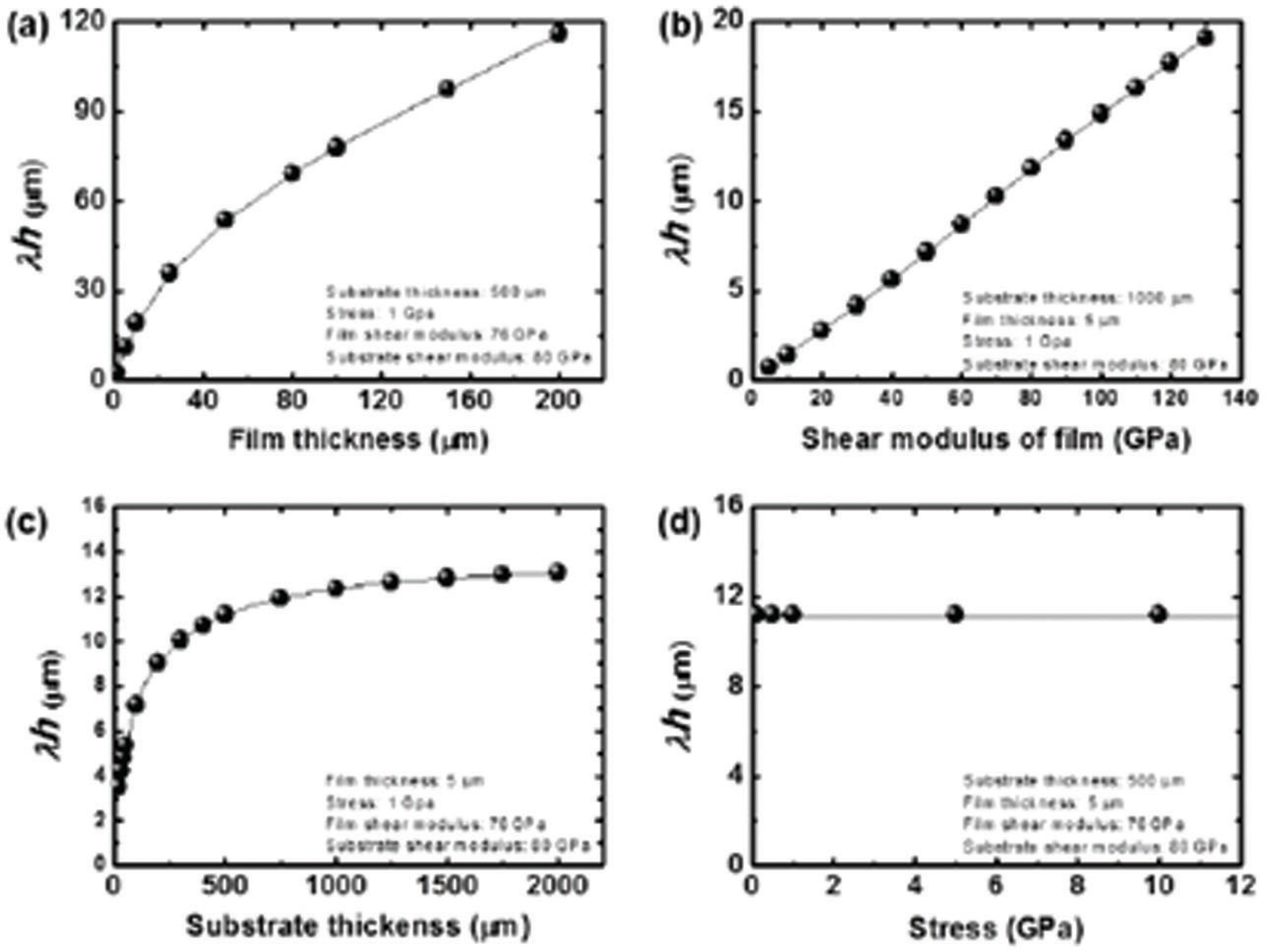
ĻĘĀņŚ┤ ĻĖ░ļ░ś ļ░Ģļ¦ē ļČäļ”¼ ĻĖ░ņłĀņØś ņĪ░Ļ▒┤ņŚÉ ļö░ļźĖ ļ░Ģļ”¼ļÉśļŖö ļ░Ģļ¦ēņØś ļæÉĻ╗ś(╬╗h)12)
2-2 ņØæļĀź ļ░£ņāØņĖĄ ĒśĢņä▒ ĻĖ░ņłĀ
ņØæļĀź ļ░£ņāØņĖĄņØĆ spalling ļ¬©ļō£ ĒīīĻ┤┤ņŚÉņä£, ĻĘĀņŚ┤ ņä▒ņןĻ│╝ ņ£äņ╣śļź╝ Ļ▓░ņĀĢĒĢśļŖöļŹ░ ņŻ╝ņÜöĒĢ£ ņŚŁĒĢĀņØä ĒĢ£ļŗż. ņØæļĀź ļ░£ņāØņĖĄņØĆ spalling Ļ│ĄņĀĢ ņØ┤Ēøä Ļ╣©ņ¦ĆĻĖ░ ņē¼ņÜ┤ ļ░śļÅäņ▓┤ ļ░Ģļ¦ēņØś ņøÉņ╣ś ņĢŖļŖö ĒīīņåÉņØä ļ░®ņ¦ĆĒĢśĻĖ░ ņ£äĒĢ£ ĒĢĖļōżļ¦ü ņĖĄņ£╝ļĪ£ ņ£ĀņÜ®ĒĢĀ ņłś ņ׳ņ£╝ļ®░, ņØæļĀź ļ░£ņāØ ņĖĄņØ┤ ĻĖłņåŹņØĖ Ļ▓ĮņÜ░ ĒĢśļČĆ ņĀäĻĘ╣ņ£╝ļĪ£ ņé¼ņÜ®ĒĢśĻĖ░ ņÜ®ņØ┤ĒĢśļŗż. ņØ┤ļ¤¼ĒĢ£ ņØ┤ņ£ĀļĪ£ ĻĘĀņŚ┤ ĻĖ░ļ░ś ļ░Ģļ”¼ Ļ│ĄņĀĢņŚÉņä£ ņĀüņĀłĒĢ£ ņØæļĀź ļ░£ņāØņĖĄ ņ×¼ļŻīļź╝ ņäĀĒāØĒĢśļŖö Ļ▓āņØ┤ ņżæņÜöĒĢśļŗż. ņØæļĀź ļ░£ņāØ ņĖĄņØĆ ļŗżņØīĻ│╝ Ļ░ÖņØ┤ (1) ļåÆņØĆ ĒīīĻ┤┤ ņØĖņä▒, (2) ņåÉņē¼ņÜ┤ ņØæļĀź Ēü¼ĻĖ░ ņĀ£ņ¢┤, (3) ļ░śļÅäņ▓┤ ļ¬©ĻĖ░ĒīÉĻ│╝ņØś Ļ░ĢĒĢ£ ņĀæņ░®ļĀź, (4) ļé«ņØĆ ņ”Øņ░® ļ╣äņÜ® ņĪ░Ļ▒┤ņØä ĒĢäņÜöļĪ£ ĒĢ£ļŗż.
ļŗłņ╝ł (nickel, Ni)ņØĆ ļåÆņØĆ ĒīīĻ┤┤ ņØĖņä▒ (145-222 MPa ŌłÜm)ņØä ļ│┤ņ£ĀĒĢśĻ│Ā ņ׳ņ£╝ļ®░, ņŖżĒŹ╝Ēä░ļ¦ü ļśÉļŖö ņĀäĻĖ░ļÅäĻĖł Ļ│ĄņĀĢņØä ĒåĄĒĢ┤ ņØæļĀź Ēü¼ĻĖ░ļź╝ ņåÉņēĮĻ▓ī ņĀ£ņ¢┤ĒĢĀ ņłś ņ׳ĻĖ░ ļĢīļ¼ĖņŚÉ ņØæļĀź ļ░£ņāØņĖĄņ£╝ļĪ£ ņĀüĒĢ®ĒĢ£ Ēøäļ│┤ ļ¼╝ņ¦łļĪ£ ņé¼ņÜ®ļÉśĻ│Ā ņ׳ļŗż.13) ņśłļź╝ ļōżņ¢┤ ņŖżĒŹ╝Ēä░ļ¦ü Ļ│ĄņĀĢņØä ĒåĄĒĢ┤ ņ”Øņ░®ļÉ£ ļŗłņ╝ł ļ░Ģļ¦ēņØä ņ”Øņ░® ņŗ£, ņŖżĒŹ╝Ēä░ļ¦ü ņĢĢļĀźņØä ņĪ░ņĀłĒĢśņŚ¼ 300 ŌĆō 700 MPa ņØś ņØĖņן ņØæļĀźņØ┤ ņĪ┤ņ×¼ĒĢśļŖö ņØæļĀź ļ░£ņāØņĖĄņØä ĒśĢņä▒ĒĢĀ ņłś ņ׳ļŗż.14) ļśÉĒĢ£, ņ¦äĻ│Ą Ļ│ĄņĀĢņØ┤ ĒĢäņÜöĒĢ£ ņŖżĒŹ╝Ēä░ļ¦ü ļ░®ļ▓ĢņŚÉ ļ╣äĒĢ┤, Ļ│ĄņĀĢ ļ╣äņÜ®ņØ┤ ņāüļīĆņĀüņ£╝ļĪ£ ņĀĆļĀ┤ĒĢśĻ│Ā ļ╣Āļź┤Ļ▓ī ļ░Ģļ¦ēņØä ĒśĢņä▒ĒĢĀ ņłś ņ׳ļŖö ņĀäĻĖ░ļÅäĻĖł ļ░®ļ▓ĢņØä ņé¼ņÜ®ĒĢśņŚ¼ ļåÆņØĆ ņāØņé░ņä▒ņØä Ļ░Ćņ¦ĆļŖö ļŗłņ╝ł ņØæļĀź ļ░£ņāØņĖĄņØä ĒśĢņä▒ĒĢĀ ņłśļÅä ņ׳ļŗż. ņĀäĻĖ░ļÅäĻĖłņØä ĒåĄĒĢ┤ ĒśĢņä▒ļÉśļŖö ļŗłņ╝łņĖĄņØś ņØæļĀźņØĆ ļČłņł£ļ¼╝, Ļ▓░ĒĢ©, grain size ļō▒ ņŚÉ ņØśĒĢ┤ņä£ Ļ▓░ņĀĢļÉśļ®░, ņØ┤ļ¤¼ĒĢ£ ņÜöņåīļōżņØĆ ņĀäĻĖ░ļÅäĻĖł Ļ│ĄņĀĢņŚÉņä£ ņé¼ņÜ®ļÉśļŖö ņĀäĒĢ┤ņ¦łņØś ĒÖöĒĢÖņĀü ņĪ░ņä▒Ļ│╝ ļÅÖņ×æ ņĀäļźś ļ░ĆļÅäņŚÉ ņśüĒ¢źņØä ļ░øļŖöļŗż.15) ņśłļź╝ ļōżļ®┤, ļé«ņØĆ ļÅÖņ×æ ņĀäļźś ļ░ĆļÅä (<15 mA/cm2)ņŚÉņä£ļŖö ņĢĢņČĢ ņØæļĀźņØś ļŗłņ╝ł ļ░Ģļ¦ēņØ┤ ĒśĢņä▒ļÉśļŖö ļ░śļ®┤, ņØ┤ļ│┤ļŗż ļåÆņØĆ ļÅÖņ×æ ņĀäļźś ļ░ĆļÅäņŚÉņä£ļŖö ņØĖņן ņØæļĀźņØä Ļ░Ćņ¦ĆļŖö ļŗłņ╝ł ļ░Ģļ¦ēņØä ĒśĢņä▒ĒĢĀ ņłś ņ׳ļŗż.16)
Ēā£ņ¢æņĀäņ¦Ć ņĀ£ņ×æ ņŗ£ ņé¼ņÜ®ļÉśļŖö ņŖżĒü¼ļ”░ ņØĖņćä ļ░®ļ▓ĢņØä ĒåĄĒĢ┤ ņĢīļŻ©ļ»ĖļŖä (aluminium, Al) ļ░Å ņØĆ (silver, Ag) ĻĖ░ļ░śņØś ņØæļĀź ļ░£ņāØņĖĄ ĒśĢņä▒ļÅä Ļ░ĆļŖźĒĢśļŗż.17) ņŖżĒü¼ļ”░ ņØĖņćä (screen printing) ļ░®ļ▓ĢņØĆ ĻĖ░ņĪ┤ņØś Ēā£ņ¢æ ņĀäņ¦Ć ņĀ£ņĪ░ ļ░®ņŗØņŚÉņä£ ņé¼ņÜ®ļÉśĻĖ░ ļĢīļ¼ĖņŚÉ ļ│äļÅäņØś ņןļ╣ä ņäżņ╣śņŚåņØ┤ ņé¼ņÜ®ņØ┤ Ļ░ĆļŖźĒĢśļŗż. ĻĘĖļ¤¼ļéś ĻĘĀņŚ┤ ĻĖ░ļ░ś ļ░Ģļ”¼ Ļ│ĄņĀĢņŚÉņä£ ĒĢäņÜöĒĢ£ ļåÆņØĆ ņØæļĀźņØä ļ░£ņāØņŗ£ĒéżĻĖ░ ņ£äĒĢ┤ņä£ļŖö ņāüļīĆņĀüņ£╝ļĪ£ Ļ│Āņś©ņØś ņŚ┤ Ļ│ĄņĀĢņØ┤ ĒĢäņÜöĒĢśļ®░, Ļ│Āņś© ņŚ┤ Ļ│ĄņĀĢņŚÉņä£ ļ░£ņāØĒĢśļŖö ĻĖłņåŹ ļČłņł£ļ¼╝ņØś ņŗżļ”¼ņĮś ļ░śļÅäņ▓┤ļĪ£ņØś ĒÖĢņé░ ļ░Å ņŗżļ”¼ņĮś Ļ│äļ®┤ņŚÉņä£ ņé░ĒÖöļ¼╝ ļ░Ģļ¦ē ĒśĢņä▒ņØĆ ļŗ©ņĀÉņ£╝ļĪ£ ņ¢ĖĻĖēļÉ£ļŗż. ņØ┤ļ┐Éļ¦ī ņĢäļŗłļØ╝, ņŗżļ”¼ņĮśņØś brittle-to-ductile ņś©ļÅä (545 Ōäā)ļ│┤ļŗż ļåÆņØĆ ņś©ļÅäņŚÉņä£ ļ░£ņāØĒĢśļŖö ĻĘĀņŚ┤ ļ░£ņāØņØĆ, ĻĘĀņŚ┤ ņäĀļŗ©ņŚÉņä£ ļ¦ēļīĆĒĢ£ ņ¢æņØś Ļ▓░ĒĢ©ņØä ļ░£ņāØņŗ£Ēé¼ ņłś ņ׳ļŗż.18)
ņ£äņŚÉņä£ ņ¢ĖĻĖēĒĢ£ ĻĖłņåŹ ĻĖ░ļ░ś ņØæļĀź ļ░£ņāØņĖĄņØś ļŗ©ņĀÉņØä Ēö╝ĒĢś Ļ│Āņ×É, ņŚ┤Ļ▓ĮĒÖöņä▒ ĒÅ┤ļ”¼ļ©Ė (thermosetting polymer) ĻĖ░ļ░śņØś ļ░Ģļ¦ēņØä ņØæļĀź ļ░£ņāØņĖĄņ£╝ļĪ£ ņé¼ņÜ®ĒĢśļĀżļŖö ņŚ░ĻĄ¼ļÅä ņ¦äĒ¢ēļÉśĻ│Ā ņ׳ļŗż. ĒÅ┤ļ”¼ļ©ĖņĖĄņØĆ ļ░śļÅäņ▓┤ ļ¬©ĻĖ░ĒīÉņŚÉ drop-castingņØ┤ļéś ņŖżĒĢĆ ņĮöĒīģ (spin coating) ļ░®ļ▓Ģņ£╝ļĪ£ ņåÉņēĮĻ▓ī ĒśĢņä▒ņØ┤ Ļ░ĆļŖźĒĢśļ®░, ĒÅ┤ļ”¼ļ©ĖņĖĄĻ│╝ ļ░śļÅäņ▓┤ Ļ░äņØś ņŚ┤ĒīĮņ░Į Ļ│äņłś ņ░©ņØ┤Ļ░Ć Ēü¼ļ»ĆļĪ£ ļé«ņØĆ ņŚ┤ Ļ│ĄņĀĢ ņś©ļÅäņŚÉņä£ļÅä ĻĘĀņŚ┤ ĻĖ░ļ░ś ļ░Ģļ”¼ Ļ│ĄņĀĢņØä ņ£äĒĢ£ ļåÆņØĆ ņØæļĀźņØ┤ ņēĮĻ▓ī ļ░£ņāØ ļÉĀ ņłś ņ׳ļŗż. Martini ļō▒ņØĆ ņØæļĀź ļ░£ņāØņĖĄņ£╝ļĪ£ ĒÅ┤ļ”¼ļ©Ėļź╝ ņé¼ņÜ®ĒĢśņŚ¼ ņŗżļ”¼ņĮś ļ¬©ĻĖ░ĒīÉņŚÉ ļ░Ģļ”¼ Ļ│ĄņĀĢņØä ņłśĒ¢ēĒĢśņśĆņ£╝ļ®░, Ōł╝100 ╬╝m ņØ┤ĒĢś ļæÉĻ╗śņØś ļ░ĢĒśĢ ņŗżļ”¼ņĮś ĻĖ░ĒīÉ ņĀ£ņ×æņØä ļ│┤Ļ│ĀĒĢśņśĆļŗż.19) ĻĘĖļ¤¼ļéś ĒÅ┤ļ”¼ļ©Ė ĻĖ░ļ░ś ņØæļĀź ļ░£ņāØņĖĄ ļæÉĻ╗śņØś ļé«ņØĆ ĻĘĀņØ╝ņä▒ņ£╝ļĪ£ ņØĖĒĢ┤, ļ░Ģļ”¼ļÉ£ ņŗżļ”¼ņĮś ĻĖ░ĒīÉņØś ļæÉĻ╗śņØś ĒÄĖņ░©Ļ░Ć ļåÆņØĆ ļŗ©ņĀÉņØĆ ĒĢ┤Ļ▓░ĒĢ┤ņĢ╝ ĒĢĀ Ļ│╝ņĀ£ļĪ£ ļé©ņĢä ņ׳ļŗż.
2-3 ĻĘĀņŚ┤ ņ¦äņĀä ļ░®ļ▓Ģ
ĻĘĀņŚ┤ ĻĖ░ļ░ś ļ░Ģļ”¼ Ļ│ĄņĀĢņØä ņłśĒ¢ēĒĢśĻĖ░ ņ£äĒĢ┤ņä£ļŖö, ņØæļĀź ļ░£ņāØņĖĄņ£╝ļĪ£ļČĆĒä░ ņ£ĀļÅäļÉśļŖö ļ¬©ĻĖ░ĒīÉņØś ĻĘĀņŚ┤ ņä▒ņן ņĪ░Ļ▒┤(G > G c)ņØä ļ¦īņĪ▒ĒĢ┤ņĢ╝ ĒĢ£ļŗż. ĻĘĀņŚ┤ ĻĖ░ļ░ś ļ░Ģļ¦ē ļ░Ģļ”¼ Ļ│ĄņĀĢņØä ņŗżĒśäĒĢśļŖö Ļ░Ćņן ņåÉņē¼ņÜ┤ ļ░®ļ▓ĢņØś ĒĢśļéśļŖö G Ļ░ÆņØä ņ”ØĻ░Ćņŗ£ĒéżĻĖ░ ņ£äĒĢ┤ ņØæļĀź ļ░£ņāØņĖĄņØä ļæÉĻ╗ŹĻ▓ī ĒśĢņä▒ĒĢśļŖö Ļ▓āņØ┤ļŗż (ņŗØ 1 ņ░ĖņĪ░).
ļśÉ ļŗżļźĖ ņĀæĻĘ╝ ļ░®ļ▓Ģņ£╝ļĪ£ļŖö, ņØæļĀź ļ░£ņāØņĖĄĻ│╝ ļ░śļÅäņ▓┤ ļ¬©ĻĖ░ĒīÉĻ│╝ņØś ņŚ┤ĒīĮņ░Į Ļ│äņłśĻ░Ć ļŗżļźĖ ņĀÉņØä ņØ┤ņÜ®ĒĢśļŖö Ļ▓āņØ┤ļŗż. ņśłļź╝ ļōżņ¢┤, ļŗłņ╝łĻ│╝ Ļ░ÖņØĆ ĻĖłņåŹ ņØæļĀźņĖĄņØĆ ņŗżļ”¼ņĮś ļ░śļÅäņ▓┤ ĻĖ░ĒīÉļ│┤ļŗż ņŚ┤ĒīĮņ░Į Ļ│äņłśĻ░Ć ļåÆļŗż (Ni: 13 ppm/Ōäā, Si: 2.6 ppm/Ōäā).20) ļŗłņ╝ł ĻĖ░ļ░ś ņØæļĀź ļ░£ņāØņĖĄņØä ņŗżļ”¼ņĮś ļ¬©ĻĖ░ĒīÉņ£äņŚÉ ĒśĢņä▒ Ēøä ņŚ┤ Ļ│ĄņĀĢņØä ņ¦äĒ¢ēĒĢśĻ▓ī ļÉśļ®┤, ļŗłņ╝łĻ│╝ ņŗżļ”¼ņĮś ļ¬©ĻĖ░ĒīÉņØś ņŚ┤ĒīĮņ░Į Ļ│äņłś ņ░©ņØ┤ļĪ£ ņØĖĒĢ┤ ļåÆņØĆ ņØæļĀźņØ┤ ļ░£ņāØĒĢśĻ│Ā ņØ┤ļĪ£ ņØĖĒĢ┤ ņŗżļ”¼ņĮś ĻĖ░ĒīÉņŚÉ ĻĘĀņŚ┤ņØ┤ ļ░£ņāØĒĢśĻ▓ī ļÉ£ļŗż. ņØ┤ļĢī, ļĀłņØ┤ņĀĆ ņ¢┤ļĖöļĀłņØ┤ņģś (laser ablation) ļ░®ļ▓ĢņØä ņØ┤ņÜ®ĒĢśņŚ¼ ņ┤łĻĖ░ ĻĘĀņŚ┤ ĒśĢņä▒ ņØä ĒåĄĒĢ┤ ĻĘĀņŚ┤ ļ░£ņāØ ņŗ£ņ×æņĀÉ ļ░Å ļ░£ņāØ ļ░®Ē¢źņØä ņĀ£ņ¢┤ĒĢĀ ņłś ņ׳ļŗż.21)
ņĄ£ĻĘ╝ņŚÉ Bedell ļō▒ņØĆ ņāłļĪ£ņÜ┤ ņĀ£ņ¢┤ļÉ£ ņŖżĒÅ┤ļ¦ü Ļ│ĄņĀĢ(controlled spalling process) ļ░®ļ▓ĢņØä ļ│┤Ļ│ĀĒĢśņśĆļŗż.14,22) ņĀ£ņ¢┤ļÉ£ ņŖżĒÅ┤ļ¦ü Ļ│ĄņĀĢ ĻĖ░ņłĀņØĆ ņØæļĀź ļ░£ņāØņĖĄņØä ĒśĢņä▒ĒĢ£ ņØ┤Ēøä, ņÖĖļČĆņŚÉņä£ ļ░£ņāØĒĢśļŖö ĻĖ░Ļ│äņĀü ņÖĖļĀźņØä ĒåĄĒĢ£ ĻĘĀņŚ┤ ņ¦äņĀä ļ░Å ņØ┤ļź╝ ĒåĄĒĢ£ ļ░śļÅäņ▓┤ ļ░Ģļ¦ē ļČäļ”¼Ļ░Ć Ļ░ĆļŖźĒĢ©ņØä ļ│┤ņŚ¼ņŻ╝ņŚłļŗż. Fig. 5ļŖö ņĀ£ņ¢┤ļÉ£ ņŖżĒÅ┤ļ¦ü Ļ│ĄņĀĢ ļ░®ļ▓ĢņØä Ļ░£ļץņĀüņ£╝ļĪ£ ļ│┤ņŚ¼ ņżĆļŗż. ņĀ£ņ¢┤ļÉ£ ņŖżĒÅ┤ļ¦ü Ļ│ĄņĀĢņØä ņłśĒ¢ēĒĢśĻĖ░ ņ£äĒĢ┤ņä£ļŖö, ļ©╝ņĀĆ ļ░śļÅäņ▓┤ ļ¬©ĻĖ░ĒīÉņŚÉ ļŗłņ╝ł ĻĖ░ļ░śņØś ņØæļĀź ļ░£ņāØņĖĄņØä ĒśĢņä▒ĒĢ£ļŗż.23) ņØ┤ļĢī ļŗłņ╝ł ĻĖ░ļ░ś ņØæļĀź ļ░£ņāØņĖĄņØś ļæÉĻ╗śņÖĆ ņØæļĀź Ēü¼ĻĖ░ņØś ļ»ĖņäĖĒĢ£ ņĀ£ņ¢┤ļź╝ ĒåĄĒĢ┤, ņ×Éļ░£ņĀüņØĖ ņŖżĒÅ┤ļ¦ü ļ¬©ļō£ ĒīīĻ┤┤ ņśüņŚŁņŚÉ ņ¦äņ×ģĒĢśĻĖ░ ņ¦üņĀä ņĪ░Ļ▒┤ņ£╝ļĪ£ ņØæļĀź ļ░£ņāØņĖĄņØä ĒśĢņä▒ĒĢ£ļŗż. ļŗżņØīņ£╝ļĪ£, ņ£ĀņŚ░ ņĀæņ░®ĒģīņØ┤Ēöäļź╝ ļŗłņ╝ł ņØæļĀź ļ░£ņāØņĖĄ ņ£äņŚÉ ļČĆņ░®ĒĢ£ Ēøä ņ£ĀņŚ░ ņĀæņ░®ĒģīņØ┤Ēöäļź╝ ņ£äļĪ£ ļŗ╣ĻĖ░ļŖö ļ░®ņŗØņ£╝ļĪ£ ņČöĻ░ĆņĀüņØĖ ņØæļĀźņØä ļ░śļÅäņ▓┤ ĻĖ░ĒīÉņŚÉ ļ░£ņāØņŗ£Ēé©ļŗż. ņØ┤ļĢī ņČöĻ░ĆļĪ£ ļ░£ņāØļÉ£ ņØæļĀźņØä ĒåĄĒĢ┤ ļ░śļÅäņ▓┤ ļ¬©ĻĖ░ĒīÉņØś ĻĘĀņŚ┤ ņ¦äņĀä ņĪ░Ļ▒┤ ’╝łG > G c) ņØ┤ ņä▒ļ”ĮļÉśĻ│Ā, ņØ┤ļĪ£ ņØĖĒĢ┤ ļŗłņ╝ł ņØæļĀź ļ░£ņāØņĖĄ ņĢäļלņØś ļ░śļÅäņ▓┤ ĻĖ░ĒīÉņŚÉ ņ┤łĻĖ░ ĻĘĀņŚ┤ņØ┤ ļ░£ņāØ ļÉ£ļŗż. ņØ┤ĒøäņŚÉļÅä ņ¦ĆņåŹņĀüņ£╝ļĪ£ ņĀæņ░®ĒģīņØ┤Ēöäļź╝ ņ£äļĪ£ ļŗ╣Ļ▓©, ļ░śļÅäņ▓┤ ļ¬©ĻĖ░ĒīÉ ļé┤ļČĆņØś ņ┤łĻĖ░ ĻĘĀņŚ┤ņØ┤ ļ░śļīĆņ¬Į Ļ░Ćņןņ×Éļ”¼ ņ£äņ╣śļĪ£ ņĀäĒīīļÉśņ¢┤ Ļ▓░ĻĄŁņŚÉļŖö ņāüļČĆ ļ░śļÅäņ▓┤ņĖĄņØä ļ¬©ĻĖ░ĒīÉņ£╝ļĪ£ļČĆĒä░ ņÖäņĀäĒ׳ ļ░Ģļ”¼ņŗ£Ēé©ļŗż. ņĀ£ņ¢┤ļÉ£ ņŖżĒÅ┤ļ¦ü ĻĖ░ņłĀņØĆ ņÖĖļČĆņŚÉņä£ ļ░£ņāØĒĢ£ ĻĖ░Ļ│äņĀü ņØæļĀźņØä ĒåĄĒĢ┤ ņ┤łĻĖ░ ĻĘĀņŚ┤ ļ░£ņāØ ņ£äņ╣ś, ĻĘĀņŚ┤ ņĀäĒīī ļ░®Ē¢ź ņĀ£ņ¢┤ ļ░Å ņåÉņē¼ņÜ┤ ĻĘĀņŚ┤ ņĀäĒīīĻ░Ć Ļ░ĆļŖźĒĢ£ Ļ▓āņØä ļ│┤ņŚ¼ ņŻ╝ņŚłļŗż. ļśÉĒĢ£ ņØ┤ļ¤¼ĒĢ£ ļ░®ļ▓ĢņØĆ ļĀłņØ┤ņĀĆ ņ¢┤ļĖöļĀłņØ┤ņģśĻ│╝ Ļ░ÖņØĆ ņĀĢĻĄÉĒĢ£ ĻĘĀņŚ┤ ļ░£ņāØ ņןļ╣ä ņŚåņØ┤ļÅä ļ░Ģļ¦ē ļ░Ģļ”¼Ļ░Ć Ļ░ĆļŖźĒĢśļ»ĆļĪ£ ņé░ņŚģņĀüņ£╝ļĪ£ ĒÜ©ņÜ® Ļ░Ćņ╣śĻ░Ć ļåÆļŗżĻ│Ā ĒĢĀ ņłś ņ׳Ļ▓Āļŗż.
Fig.┬Ā5.
ņĀ£ņ¢┤ļÉ£ ņŖżĒÅ┤ļ¦ü Ļ│ĄņĀĢ (controlled spalling process) ļ░®ļ▓ĢņØä ņØ┤ņÜ®ĒĢ£ ļ░Ģļ¦ē ļČäļ”¼ ĻĖ░ņłĀ ļ¬©ņŗØļÅä[23]

2-4 ļŗżņ¢æĒĢ£ ļ░śļÅäņ▓┤ ĻĖ░ĒīÉņŚÉ ņĀüņÜ®ļÉ£ ĻĘĀņŚ┤ ĻĖ░ļ░ś ļ░Ģļ”¼ ĻĖ░ņłĀ
ļŗżļźĖ ļ░Ģļ¦ē ļČäļ”¼ ĻĖ░ņłĀĻ│╝ ļ╣äĻĄÉĒĢśņŚ¼, ĻĘĀņŚ┤ ĻĖ░ļ░ś ļ░Ģļ¦ē ļČäļ”¼ ļ░®ļ▓ĢņØś ņןņĀÉņØĆ ļŗżņ¢æĒĢ£ ļ░śļÅäņ▓┤ (ņśł: Si, Ge, GaAs, InP, GaN) ĻĖ░ĒīÉņŚÉ ļ▓öņÜ®ņĀüņ£╝ļĪ£ ņĀüņÜ®ĒĢĀ ņłś ņ׳ļŖö Ļ▓āņØ┤ļŗż. ļ░śļÅäņ▓┤ ĻĖ░ĒīÉņØś ĻĘĀņŚ┤ ĻĖ░ļ░ś ļ░Ģļ¦ē ļČäļ”¼ ĻĖ░ņłĀ ņłśĒ¢ē ņŗ£ Ļ│ĀļĀżĒĢ┤ņĢ╝ ĒĢśļŖö Ļ░Ćņן ņżæņÜöĒĢ£ ņ×¼ļŻī ĒŖ╣ņä▒ ņżæ ĒĢśļéśļŖö ļ░śļÅäņ▓┤ ļ¬©ĻĖ░ĒīÉņØś G c ņØ┤ļŗż. ĒŖ╣ņĀĢ ļ░śļÅäņ▓┤ ĻĖ░ĒīÉņŚÉ ĻĘĀņŚ┤ ĻĖ░ļ░ś ļ░Ģļ¦ē ļČäļ”¼ ĻĖ░ņłĀņØä ņĀüņÜ®ĒĢĀ ņŗ£, ļ░śļÅäņ▓┤ ļ¬©ĻĖ░ĒīÉņØś G c Ļ░ÆņØä Ļ│ĀļĀżĒĢśņŚ¼ ņØæļĀź ļ░£ņāØņĖĄņØś ņØæļĀźĻ│╝ ļæÉĻ╗śļź╝ ņĄ£ņĀüĒÖöņŗ£Ēé¼ ĒĢäņÜöĻ░Ć ņ׳ļŗż.
ņŗżļ”¼ņĮś (silicon, Si) ņØĆ Ēā£ņ¢æ ņĀäņ¦Ć ļ░Å ņĀäņ×É ņåīņ×É ņé░ņŚģņŚÉņä£ Ļ░Ćņן ļ▓öņÜ®ņĀüņ£╝ļĪ£ ņé¼ņÜ®ļÉśļŖö ļ░śļÅäņ▓┤ ņ×¼ļŻīņØ┤ļŗż. ņĄ£ĻĘ╝ņŚÉļŖö ĻĘĀņŚ┤ ĻĖ░ļ░ś ļ░Ģļ”¼ ĻĖ░ņłĀņØä ņØ┤ņÜ®ĒĢśņŚ¼, ņø©ņØ┤ĒŹ╝ ņŖżņ╝ĆņØ╝ (> 4ņØĖņ╣ś) Ļ▓░ņĀĢņ¦ł ņŗżļ”¼ņĮś ĻĖ░ļ░śņØś ņ£ĀņŚ░ Ēā£ņ¢æ ņĀäņ¦Ć ļ░Å ņĀäņ×É ņåīņ×É ņĀ£ņ×æņŚÉ ļīĆĒĢ£ ļ│┤Ļ│ĀĻ░Ć ļÉśĻ│Ā ņ׳ļŗż. Fig. 6ņØĆ 500 ╬╝ m ļæÉĻ╗śņØś ņŗżļ”¼ņĮś ļ¬©ĻĖ░ĒīÉņŚÉņä£ ļ░Ģļ”¼ļÉ£ 50 ╬╝m ļ»Ėļ¦īņØś ļæÉĻ╗śņØś ļ¦żļüäļ¤¼ņÜ┤ Ēæ£ļ®┤ņØä Ļ░Ćņ¦ĆļŖö Ļ▓░ņĀĢņ¦ł ņŗżļ”¼ņĮś ļ░Ģļ¦ēņØä ļ│┤ņŚ¼ ņżĆļŗż.24) Free-standing ņŗżļ”¼ņĮś ļ░Ģļ¦ēņØĆ ĻĖ░Ļ│äņĀüņ£╝ļĪ£ ņĘ©ņĢĮĒĢśņ¦Ćļ¦ī, ĻĘĀņŚ┤ ņ¦äņĀä ĻĖ░ļ░ś ļ░Ģļ¦ē ļČäļ”¼ Ļ│ĄņĀĢņŚÉ ņØśĒĢ┤ ņĀ£ņ×æļÉ£ ļ░Ģļ¦ē ņŗżļ”¼ņĮś/ĻĖłņåŹ ņØæļĀź ļ░£ņāØņĖĄ ĻĄ¼ņĪ░ļŖö ĻĖ░Ļ│äņĀüņ£╝ļĪ£ Ļ▓¼Ļ│ĀĒĢśņŚ¼ ņÖĖļČĆ ņČ®Ļ▓®ņ£╝ļĪ£ ņØĖĒĢ┤ ņל Ļ╣©ņ¦Ćņ¦Ć ņĢŖļŖö ņןņĀÉņØ┤ ņ׳ļŗż. ļśÉĒĢ£ ĻĘĀņŚ┤ ĻĖ░ļ░ś ļ░Ģļ¦ē ļČäļ”¼ ĻĖ░ņłĀņØĆ ņĢ×ņŚÉņä£ ņ¢ĖĻĖēĒĢ£ ļŹ░ļĪ£, ļ░śļÅäņ▓┤ ļ░Ģļ¦ē ļČäļ”¼ ņŗ£ ņ¢┤ļ¢ĀĒĢ£ ņ×¼ļŻī ņåÉņŗżļÅä ļ░£ņāØĒĢśņ¦Ć ņĢŖņØīņ£╝ļĪ£ Ļ▓ĮņĀ£ņä▒ ņ׳ļŖö ņø©ņØ┤ĒŹ╝ļ¦ü ĻĖ░ņłĀļĪ£ ļ░£ņĀäĒĢĀ Ļ░ĆļŖźņä▒ņØ┤ Ēü¼ļŗżĻ│Ā ļ│╝ ņłś ņ׳Ļ▓Āļŗż. ņØ┤ļŖö, ļ░śļÅäņ▓┤ ĻĖ░ĒīÉņØś ņĀ£ņ×æ ļ╣äņÜ®ņØś Ļ░ÉņåīĻ░Ć ņżæņÜöĒĢ£ Ēā£ņ¢æ ņĀäņ¦Ć ņé░ņŚģņŚÉ Ēü░ ņØ┤ņĀÉņ£╝ļĪ£ ņ×æņÜ®ĒĢĀ ņłś ņ׳ļŗż. ņĄ£ĻĘ╝ņŚÉļŖö ĒĢśļéśņØś Ļ▓░ņĀĢņ¦ł ņŗżļ”¼ņĮś ļ¬©ĻĖ░ĒīÉņŚÉņä£ ņŚ░ņåŹņĀüņØĖ ĻĘĀņŚ┤ ĻĖ░ļ░ś ļ░Ģļ¦ē ļČäļ”¼ ĻĖ░ņłĀņØä ņłśĒ¢ēĒĢśņŚ¼, ņŚ¼ļ¤¼ Ļ░£ņØś Si ļ░Ģļ¦ē ņāØņé░ Ļ░ĆļŖźĒĢ©ņØä ļ│┤ņŚ¼ ņŻ╝ņŚłļŗż (Fig. 6 (d)). ļ░ĢĒśĢ ļ░śļÅäņ▓┤ ĻĖ░ĒīÉņØś Ēæ£ļ®┤ Ļ▒░ņ╣ĀĻĖ░ļŖö ļ░Ģļ”¼ Ļ│ĄņĀĢņØ┤ ņ¦äĒ¢ēĒĢ©ņŚÉ ļö░ļØ╝ ņł£ņ░©ņĀüņ£╝ļĪ£ ņ”ØĻ░ĆĒĢśņŚ¼ ņäĖ ļ▓łņ¦ĖļĪ£ ņĀ£ņ×æļÉ£ Si ļ░Ģļ¦ēņØś Ļ▓ĮņÜ░ 312 nmņŚÉņä£ 459 nmļĪ£ ņ”ØĻ░ĆĒĢśņśĆļŗż. ĒĢśņ¦Ćļ¦ī, ņØ┤ļ¤¼ĒĢ£ Ēæ£ļ®┤ Ļ▒░ņ╣ĀĻĖ░ļŖö ĻĖ░ņĪ┤ņØś ļŗżņżæ ņÖĆņØ┤ņ¢┤ ņÅśņ×ē ĻĖ░ļ▓ĢņØś ņø©ņØ┤ĒŹ╝ļ¦ü ĻĖ░ņłĀņŚÉ ļ╣äĒĢśļ®┤ ņŚ¼ņĀäĒ׳ ļ¦żņÜ░ ļé«ņØĆ Ļ░ÆņØ┤ļŗż. ļśÉĒĢ£ ņ£äņŚÉņä£ ņ¢ĖĻĖēĒĢ£ ļ░öņÖĆ Ļ░ÖņØ┤, ĻĘĀņŚ┤ ĻĖ░ļ░ś ļ░Ģļ¦ē ļČäļ”¼ ĻĖ░ņłĀņØĆ ņØæļĀź ļ░£ņāØņĖĄņØś ļæÉĻ╗ś ļ░Å ĻĖ░Ļ│äņĀü ĒŖ╣ņä▒ ņĀ£ņ¢┤ļź╝ ĒåĄĒĢ┤ ļ░Ģļ”¼ļÉśļŖö ļ░śļÅäņ▓┤ ļæÉĻ╗ś ņĀ£ņ¢┤Ļ░Ć Ļ░ĆļŖźĒĢśļŗż. Fig. 7ļŖö ļŗłņ╝ł ĻĖ░ļ░ś ņØæļĀź ļ░£ņāØņĖĄ ļæÉĻ╗śļź╝ ņĪ░ņĀłĒĢśņŚ¼ ļ░Ģļ”¼ļÉśļŖö ņŗżļ”¼ņĮś ļ░Ģļ¦ēņØś ļæÉĻ╗śļź╝ 4.6 ŌĆō 38 ╬╝m ļĪ£ ņĀ£ņ¢┤ļÉ£ ļ¬©ņŖĄņØä ļ│┤ņŚ¼ ņżĆļŗż.25)
Fig.┬Ā6.
ĻĘĀņŚ┤ ĻĖ░ļ░ś ļ░Ģļ¦ē ļČäļ”¼ ĻĖ░ņłĀļĪ£ ņĀ£ņ×æļÉ£ (a) ņŗżļ”¼ņĮś ļ░Ģļ¦ē, (b) ņé¼ņÜ®ļÉ£ ņŗżļ”¼ņĮś ļ¬©ĻĖ░ĒīÉ ļ░Å (c) ĒīīĻ┤┤ļÉ£ Ēæ£ļ®┤ņØś SEM (scanning electron microscope) ņØ┤ļ»Ėņ¦Ć. (d) ņŚ░ņåŹņĀüņØĖ ĻĘĀņŚ┤ ĻĖ░ļ░ś ļ░Ģļ¦ē ļČäļ”¼ ĻĖ░ņłĀļĪ£ ņĀ£ņ×æļÉ£ ņŗżļ”¼ņĮś ļ░Ģļ¦ē.24)
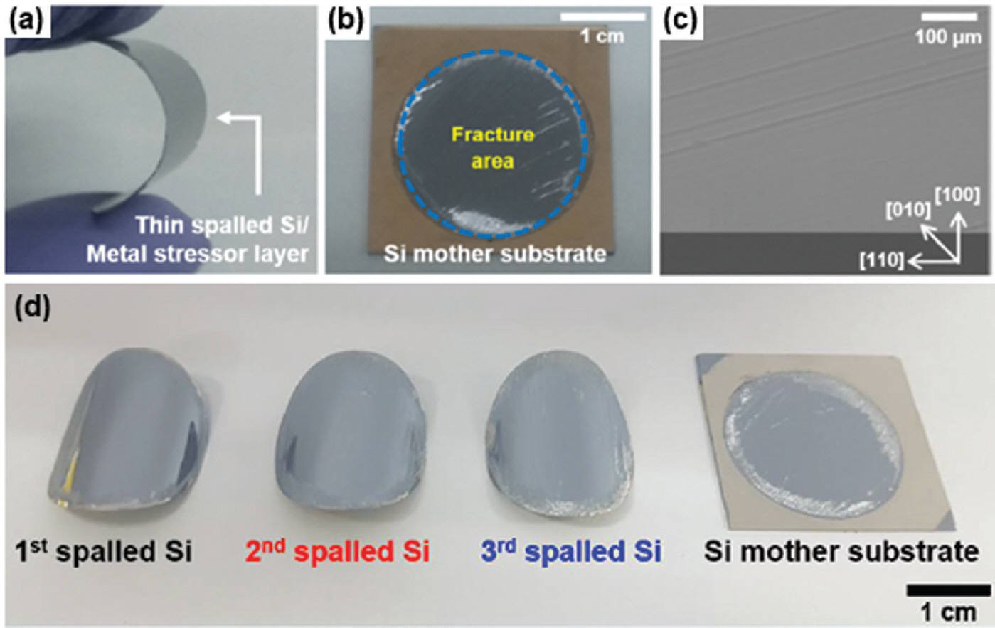
Fig.┬Ā7.
ļŗłņ╝ł ņŖżĒŖĖļĀłņŖżņĖĄ ļæÉĻ╗ś ņĀ£ņ¢┤ļź╝ ĒåĄĒĢ┤ ņĀ£ņ×æļÉ£ ļŗżņ¢æĒĢ£ ļæÉĻ╗śņØś ņŗżļ”¼ņĮś ļ░Ģļ¦ēņØś SEM ņØ┤ļ»Ėņ¦Ć.25)

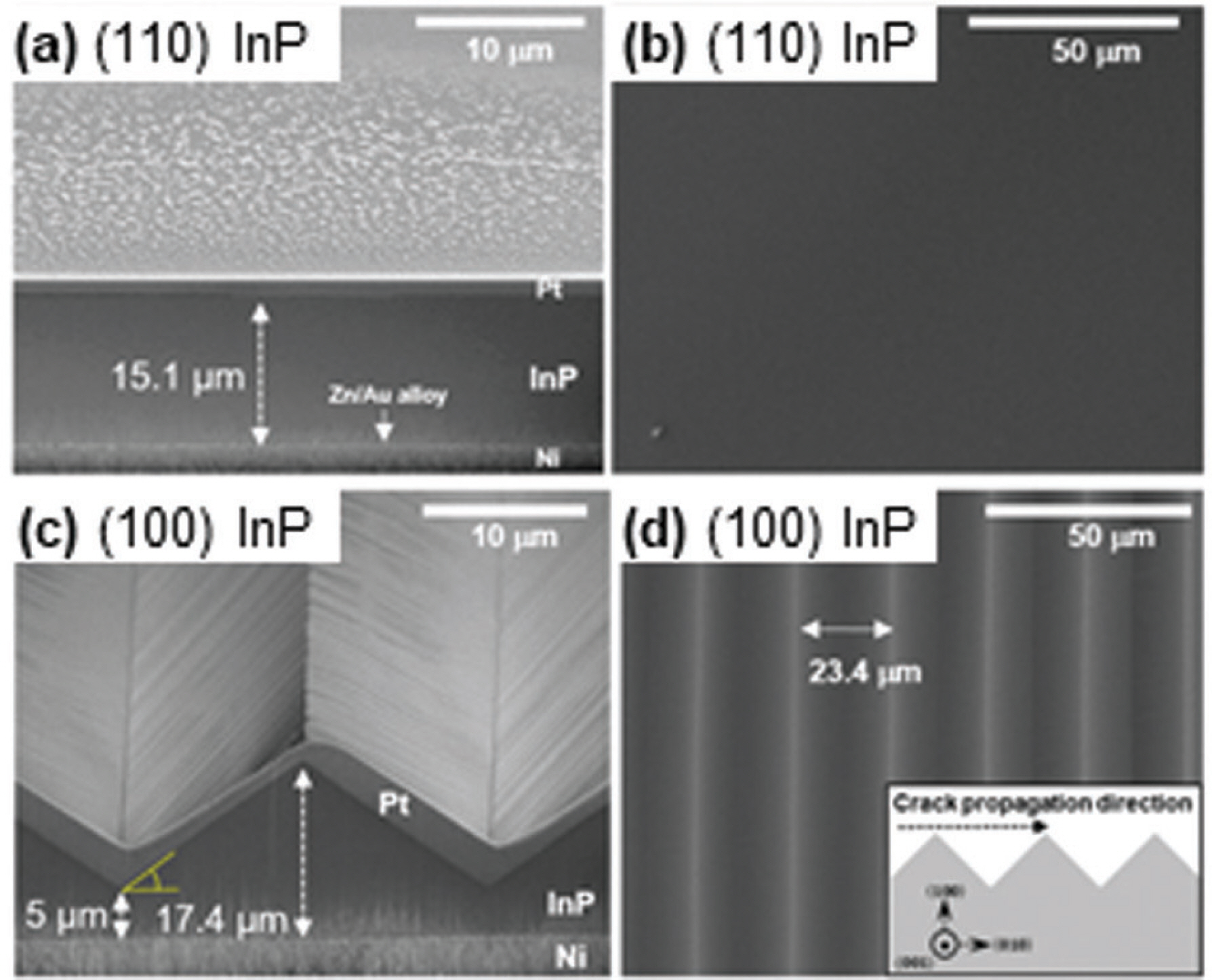
Indium phosphide (InP)ļŖö ņ¦üņĀæĒśĢ ļ░┤ļō£Ļ░Ł (direct bandgap) ņØ┤ļ®░, ļåÆņØĆ ņĀäņ×É ņØ┤ļÅÖļÅä (electron mobility, 5400cm2/V┬Ęs) ļ░Å ļé«ņØĆ Ēæ£ļ®┤ ņ×¼Ļ▓░ĒĢ® ņåŹļÅä (surface recombination velocity, 104 ŌĆō 105 cm/s)ņØä Ļ░Ćņ¦Ćļ»ĆļĪ£ Ļ┤æņĀäņ×É ņé░ņŚģņØś ņŻ╝ņÜöĒĢ£ ļ░śļÅäņ▓┤ ņ×¼ļŻī ņżæ ĒĢśļéśļØ╝ ĒĢĀ ņłś ņ׳Ļ▓Āļŗż.26,27) ņĄ£ĻĘ╝ņŚÉ ĻĘĀņŚ┤ ĻĖ░ļ░ś ļ░Ģļ¦ē ļČäļ”¼ ĻĖ░ņłĀņØä InP ĻĖ░ĒīÉņŚÉ ņĀüņÜ®ĒĢ£ InP ļ░Ģļ¦ē ņĀ£ņĪ░ ĻĖ░ņłĀņØ┤ ļ│┤Ļ│ĀļÉśņŚłļŗż (Fig. 8).28) ĻĘĀņŚ┤ ĻĖ░ļ░ś ļ░Ģļ¦ē ļČäļ”¼ ĻĖ░ņłĀņØä zinc-blende Ļ▓░ņĀĢ ĻĄ¼ņĪ░ļź╝ Ļ░Ćņ¦ĆļŖö InP ļ¬©ĻĖ░ĒīÉņŚÉ ņĀüņÜ®ĒĢĀ Ļ▓ĮņÜ░, InP ļ¬©ĻĖ░ĒīÉņØś Ļ▓░ņĀĢ ļ░®Ē¢źņŚÉ ļö░ļØ╝ ļ░Ģļ”¼ļÉśļŖö InP ļ░Ģļ¦ēņØś Ēæ£ļ®┤ ĻĄ¼ņĪ░Ļ░Ć Ēü¼Ļ▓ī ļŗ¼ļØ╝ņ¦ĆļŖö Ļ▓āņØä ļ│┤ņŚ¼ ņŻ╝ņŚłļŗż. Zinc-blende Ļ▓░ņĀĢ ĻĄ¼ņĪ░ņØś InPņØś Ļ▓ĮņÜ░ ļ░śļÅäņ▓┤ Ļ▓░ņĀĢ ļ░®Ē¢źņŚÉ ļö░ļØ╝ G c Ļ░ÆņØ┤ ļŗ¼ļØ╝ņ¦Ćļ®░, (110) ļ®┤ņŚÉņä£ Ļ░Ćņן ņ×æņØĆ G c Ļ░ÆņØä Ļ░Ćņ¦ĆĻ│Ā ņ׳ĻĖ░ ļĢīļ¼ĖņŚÉ ĻĘĀņŚ┤ ņ¦äņĀä ļ░®Ē¢źņØ┤ ņŻ╝ļĪ£ (110) ļ®┤ņŚÉ ĻĄŁĒĢ£ļÉ£ļŗż. ļö░ļØ╝ņä£ (110) ļ░®Ē¢źņØś InP ļ¬©ĻĖ░ĒīÉņŚÉ ĻĘĀņŚ┤ ĻĖ░ļ░ś ļ░Ģļ¦ē ļČäļ”¼ ĻĖ░ņłĀņØ┤ ņĀüņÜ® ņŗ£ ļ¦żņÜ░ ļ¦żļüäļ¤¼ņÜ┤ Ēæ£ļ®┤ņØä Ļ░Ćņ¦ĆļŖö InP ļ░Ģļ¦ē ņĀ£ņ×æņØ┤ Ļ░ĆļŖźĒĢśļŗż. ņØ┤ļĢī ļ░Ģļ”¼ļÉ£ (110) InP ļ░Ģļ¦ēņØś Ēæ£ļ®┤ Ļ▒░ņ╣ĀĻĖ░ļŖö Ōł╝100 pmņ£╝ļĪ£, ņé░ņŚģņŚÉņä£ ņé¼ņÜ®ĒĢśĻ│Ā ņ׳ļŖö chemical-mechanical polishing (CMP)ņ£╝ļĪ£ ņŚ░ļ¦łļÉśļŖö ņø©ņØ┤ĒŹ╝ Ēæ£ļ®┤ (Ōł╝550 pm)ņŚÉ ļ╣äĒĢ┤ņä£ ļ¦żņÜ░ ļé«ņØĆ Ļ░ÆņØä ļ│┤ņŚ¼ ņżĆļŗż. ļ░śļ®┤ņŚÉ, (100) ļ░®Ē¢źņØś InP ļ¬©ĻĖ░ĒīÉņŚÉ ĻĘĀņŚ┤ ĻĖ░ļ░ś ļ░Ģļ¦ē ļČäļ”¼ ĻĖ░ņłĀņØä ņĀüņÜ® ņŗ£ ļ░Ģļ”¼ļÉśļŖö (110) InP ļ░Ģļ¦ē Ēæ£ļ®┤ņŚÉ ņŻ╝ĻĖ░ņĀüņØĖ ņé╝Ļ░üĒśĢ Ēæ£ļ®┤ ĻĄ¼ņĪ░Ļ░Ć ĒśĢņä▒ļÉśļŖö Ļ▓āņØä ļ│╝ ņłśĻ░Ć ņ׳ļŗż. ļśÉĒĢ£, ņØæļĀź ļ░£ņāØņĖĄ ļæÉĻ╗śļź╝ ņĀ£ņ¢┤ĒĢśņŚ¼ ņŻ╝ĻĖ░ņĀüņØĖ ņé╝Ļ░üĒśĢ Ēæ£ļ®┤ ĻĄ¼ņĪ░ņØś Ēü¼ĻĖ░ ņĀ£ņ¢┤Ļ░Ć Ļ░ĆļŖźĒĢ©ņØä ņŗżĒŚśņĀüņ£╝ļĪ£ ĒÖĢņØĖĒĢśņśĆļŗż. ņØ┤ļ¤¼ĒĢ£ ĻĖ░ĒīÉ ļČäļ”¼ņÖĆ ļÅÖņŗ£ņŚÉ ļ░Ģļ”¼ļÉśļŖö ļ░Ģļ¦ēņØś Ēæ£ļ®┤ ĻĄ¼ņĪ░ļź╝ ņĀ£ņ¢┤ Ļ░ĆļŖźĒĢ£ ņןņĀÉņØĆ ĻĘĀņŚ┤ ĻĖ░ļ░ś ļ░Ģļ”¼ ĻĖ░ņłĀļ¦īņØś ļÅģĒŖ╣ĒĢ£ ĒŖ╣ņä▒ņØ┤ļØ╝ ĒĢĀ ņłś ņ׳Ļ▓Āļŗż.
Fig.┬Ā8.
ĻĘĀņŚ┤ ĻĖ░ļ░ś ļ░Ģļ¦ē ļČäļ”¼ ĻĖ░ņłĀļĪ£ ņĀ£ņ×æļÉ£ InP ļ░Ģļ¦ē. (110) InP ļ¬©ĻĖ░ĒīÉņ£╝ļĪ£ļČĆĒä░ ļ░Ģļ”¼ļÉ£ InP ļ░Ģļ¦ēņØś (a) ļŗ©ļ®┤ ļ░Å (b) Ēæ£ļ®┤ņØś SEM ņØ┤ļ»Ėņ¦Ć. (100) InP ļ¬©ĻĖ░ĒīÉņ£╝ļĪ£ļČĆĒä░ ļ░Ģļ”¼ļÉ£ InP ļ░Ģļ¦ēņØś (c) ļŗ©ļ®┤ ļ░Å (d) Ēæ£ļ®┤ņØś SEM ņØ┤ļ»Ėņ¦Ć28)
Gallium nitride (GaN)ļŖö ļ░£Ļ┤æ ņåīņ×É (light-emitting diode) ļ░Å ņĀäļĀź ņĀäņ×É ņåīņ×ÉņŚÉņä£ ļäÉļ”¼ ņé¼ņÜ®ļÉśļŖö Ļ┤æļīĆņŚŁ ļ░┤ļō£Ļ░Ł (3.4 eV)ņØä Ļ░Ćņ¦ĆļŖö ļ░śļÅäņ▓┤ņØ┤ļŗż. GaN ļŖö Ļ░ĢĒĢ£ ņØ┤ņś© Ļ▓░ĒĢ®ņØä Ļ░Ćņ¦ĆļŖö wurtzite Ļ▓░ņĀĢ ĻĄ¼ņĪ░ļĪ£ ļÉśņ¢┤ ņ׳ņ¢┤ ņé░ņä▒ ņÜ®ņĢĪņŚÉņä£ Ļ░ĢĒĢ£ ņĢłņĀĢņä▒ņØä Ļ░Ćņ¦Ćļ»ĆļĪ£, Ļ┤æņĀäĻĖ░ĒÖöĒĢÖņĀü (photoelectrochemical) ļ¼╝ļČäĒĢ┤ļź╝ ņ£äĒĢ£ photoelectrode ņŚ░ĻĄ¼ ļČäņĢ╝ņŚÉņä£ ļåÆņØĆ Ļ┤Ćņŗ¼ņØä ļ│┤ņØ┤Ļ│Ā ņ׳ļŗż. Bedell ņØĆ ņĀ£ņ¢┤ļÉ£ ņŖżĒÅ┤ļ¦ü Ļ│ĄņĀĢņØä ĒåĄĒĢ┤ [0001] ļ░®Ē¢źņØś GaN ļ¬©ĻĖ░ĒīÉņ£╝ļĪ£ļČĆĒä░ Ōł╝20 ╬╝m ļæÉĻ╗śņØś GaN ļ░Ģļ¦ēņØś ļ░Ģļ”¼Ļ░Ć Ļ░ĆļŖźĒĢ©ņØä ļ│┤ņŚ¼ ņŻ╝ņŚłļŗż.29) ņØ┤ļĢī, ļ░Ģļ”¼ļÉ£ GaN ļ░Ģļ¦ē Ēæ£ļ®┤ņŚÉ ņłśņ¦ü ļ░®Ē¢źņ£╝ļĪ£ ņłś ļ¦łņØ┤Ēü¼ļĪ£ļ»ĖĒä░ ņłśņżĆņØś ņ¦äĒÅŁ ļ│ĆĒÖöĻ░Ć Ļ┤Ćņ░░ļÉ£ļŗż. Wurtzite Ļ▓░ņĀĢ ĻĄ¼ņĪ░ņØś GaNņØś Ļ▓ĮņÜ░ m- ĒÅēļ®┤Ļ│╝ a- ĒÅēļ®┤ņØ┤ [0001] ĒÅēļ®┤ļ│┤ļŗż ņēĮĻ▓ī ĒīīĻ┤┤Ļ░Ć ļÉśĻĖ░ ļĢīļ¼ĖņŚÉ, ņĀüņĀłĒĢ£ Ļ▓░ņĀĢ ļ░®Ē¢źņØä Ļ░Ćņ¦ĆļŖö GaN ļ¬©ĻĖ░ĒīÉņØä ņé¼ņÜ®ĒĢ©ņ£╝ļĪ£ņŹ©, ļé«ņØĆ Ēæ£ļ®┤ Ļ▒░ņ╣ĀĻĖ░ņØś GaN ļ░Ģļ¦ēņØä ņĀ£ņ×æĒĢĀ ņłś ņ׳ļŖö ņŚ¼ņ¦ĆĻ░Ć ņ׳ņØä Ļ▓āņ£╝ļĪ£ ļ│┤ņŚ¼ņ¦äļŗż.
Ļ▓░ņĀĢņ¦ł ļ░ĢĒśĢ ļ░śļÅäņ▓┤ ĻĖ░ļ░ś Ēā£ņ¢æĻ┤æ ņŚÉļäłņ¦Ć ņĀäĒÖś ņåīņ×É
3-1 Ēā£ņ¢æ ņĀäņ¦Ć
Ēā£ņ¢æĻ┤æ ņé░ņŚģņŚÉņä£ ņŗżļ”¼ņĮśņØĆ ņÜ░ņłśĒĢ£ ņŚÉļäłņ¦Ć ņĀäĒÖś ĒÜ©ņ£©Ļ│╝ ņĀüņĀłĒĢ£ ļ╣äņÜ®ņ£╝ļĪ£ ņØĖĒĢ┤ Ļ░Ćņן ņŻ╝ļ¬®ļ░øļŖö ņ×¼ļŻīņØ┤ļŗż. Saha ļō▒ņØĆ ĻĘĀņŚ┤ ĻĖ░ļ░ś ļ░Ģļ”¼ ĻĖ░ņłĀņØä ĒåĄĒĢśņŚ¼ 25 ╬╝m ļæÉĻ╗śņØś ņØ┤ņóģ ņĀæĒĢ® ņŗżļ”¼ņĮś Ēā£ņ¢æ ņĀäņ¦Ć ņĀ£ņ×æņØä ņłśĒ¢ēĒĢśņśĆļŗż.30)ĻĘĀņŚ┤ ĻĖ░ļ░ś ļ░Ģļ”¼ ĻĖ░ņłĀņØä ĒåĄĒĢ┤ņä£ ĒÜŹĻĖ░ņĀüņ£╝ļĪ£ Ļ░ÉņåīĒĢ£ ņŗżļ”¼ņĮś Ļ┤æĒØĪņłśņĖĄņØś ļæÉĻ╗ś Ļ░ÉņåīņŚÉļÅä ļČłĻĄ¼ĒĢśĻ│Ā, ļ░Ģļ”¼ļÉ£ ņŗżļ”¼ņĮśņ£╝ļĪ£ ņĀ£ņ×æļÉ£ ņĄ£ņóģ ņØ┤ņóģ ņĀæĒĢ® Ēā£ņ¢æņĀäņ¦ĆļŖö Ļ░£ļ░®ĒÜīļĪ£ņĀäņĢĢ (open circuit voltage, V oc), ļŗ©ļØĮ ĒÜīļĪ£ ņĀäļźś ļ░ĆļÅä (short circuit current density, J sc), Ļ┤æņĀä ļ│ĆĒÖś ĒÜ©ņ£©ņØ┤ Ļ░üĻ░ü 580 mV, 33.6 mA/cm2, 14.9%ļź╝ ļŗ¼ņä▒ĒĢśņśĆļŗż. ļ╣äļĪØ ļ░Ģļ”¼ļÉ£ ņŗżļ”¼ņĮś ĻĖ░ļ░ś Ēā£ņ¢æ ņĀäņ¦Ć Ļ│ĄņĀĢņØ┤ ņĄ£ņĀüĒÖöļÉśņ¦Ć ņĢŖņĢä ņé░ņŚģņŚÉņä£ ņĀ£ņĪ░ļÉśļŖö Ēā£ņ¢æņĀäņ¦ĆņŚÉ ļ╣äĒĢ┤ ĒÜ©ņ£©ņØ┤ ņāüļīĆņĀüņ£╝ļĪ£ ļé«ņ¦Ćļ¦ī, ļåÆņØĆ ņ£ĀņŚ░ņä▒ņØ┤ ņ׳ļŖö 25 ╬╝m ļæÉĻ╗śņØś ņŗżļ”¼ņĮś Ēā£ņ¢æņĀäņ¦ĆļĪ£ ņĀüļŗ╣ĒĢ£ ņłśņżĆņØś ņä▒ļŖźņØä ņ¢╗ņØä ņłś ņ׳ļŖö Ļ░ĆļŖźņä▒ņØä ļ│┤ņŚ¼ ņŻ╝ņŚłļŗż.
ņĀĆ ļ╣äņÜ®ņØś ņØ┤ņóģ ņĀæĒĢ® Ēā£ņ¢æņĀäņ¦Ćļź╝ ņĀ£ņ×æĒĢśļŖö ļśÉ ļŗżļźĖ ņĀæĻĘ╝ ļ░®ņŗØņ£╝ļĪ£ļŖö 2D ņ×¼ļŻīļź╝ ņé¼ņÜ®ĒĢśļŖö ļ░®ļ▓ĢņØ┤ ņ׳ļŗż. Ahn ļō▒ņØĆ ĻĘĀņŚ┤ ĻĖ░ļ░ś ļ░Ģļ”¼ ĻĖ░ņłĀņØä ĒåĄĒĢ┤ ņĀ£ņ×æļÉ£ 35 ╬╝m ļæÉĻ╗śņØś ņŗżļ”¼ņĮśņŚÉ graphene/Al2 O3/Si ņØ┤ņóģ ņĀæĒĢ®ņØä ĒåĄĒĢ┤ ņ£ĀņŚ░ĒĢ£ Ēā£ņ¢æņĀäņ¦Ć ņĀ£ņ×æņŚÉ ņä▒Ļ│ĄĒĢśņśĆļŗż.31) ņØ┤ ņÖĖņŚÉļÅä, ļŗżņ¢æĒĢ£ ņØ┤ņóģ ņĀæĒĢ®ņØä ņ£äĒĢśņŚ¼ MoO xņÖĆ Ļ░ÖņØĆ ņé░ĒÖöļ¼╝ ĻĖ░ļ░ś ņĀäĒĢśņäĀĒāØņĖĄņØä ņĀüņÜ®ĒĢśņŚ¼ ņ£ĀņŚ░ĒĢśļ®┤ņä£ļÅä Ļ│ĀĒÜ©ņ£©ņØś ņ£ĀņŚ░ Ēā£ņ¢æņĀäņ¦Ć Ļ░£ļ░£ņØ┤ Ļ░ĆļŖźĒĢĀ Ļ▓āņ£╝ļĪ£ ĻĖ░ļīĆļÉ£ļŗż.32,33)
Ļ▓░ņĀĢņ¦ł ņŗżļ”¼ņĮś ņ×¼ļŻīņØś Ļ▓ĮņÜ░ Ļ░äņĀæĒśĢ ļ░┤ļō£Ļ░Ł (indirect bandgap) ņØ┤ļ»ĆļĪ£, Ēā£ņ¢æĻ┤æ Ļ░Ćņŗ£Ļ┤æņØś ņןĒīīņן ņśüņŚŁņŚÉņä£ņØś Ļ┤æ ĒØĪņłśņ£©ņØ┤ ņāüļīĆņĀüņ£╝ļĪ£ ļé«ļŗż. ļö░ļØ╝ņä£ ņŗżļ”¼ņĮś ļæÉĻ╗śĻ░Ć Ļ░ÉņåīĒĢśļ®┤ ņןĒīīņן ņśüņŚŁņŚÉņä£ņØś ņČ®ļČäĒĢ£ Ļ┤æ ĒØĪņłśĻ░Ć ņ¢┤ļĀżņÜ░ļ®░, ņØ┤ļŖö Ļ┤æņĀäļźś ļ░Å Ļ┤æņĀä ļ│ĆĒÖś ĒÜ©ņ£© Ļ░Éņåīļź╝ ņĢ╝ĻĖ░ĒĢ£ļŗż. ņØ┤ļ¤¼ĒĢ£ ļ¼ĖņĀ£ļź╝ ĒĢ┤Ļ▓░ĒĢśĻĖ░ ņ£äĒĢ┤ņä£ ļéśļģĖņŖżņ╝ĆņØ╝ ņŚŁĒö╝ļØ╝ļ»Ėļō£ ĻĄ¼ņĪ░ņÖĆ Ļ░ÖņØĆ ņĀüņĀłĒĢ£ Ļ┤æĒżĒÜŹ (light-trapping) ĻĄ¼ņĪ░ļź╝ ņé¼ņÜ®ĒĢśņŚ¼ Ļ┤æĒØĪņłś Ļ▓ĮļĪ£ ĻĖĖņØ┤ļź╝ ĒÖĢņןņŗ£ņ╝£, ņןĒīīņן ņśüņŚŁņŚÉņä£ņØś Ļ┤æĒØĪņłśņ£©ņØä Ē¢źņāüĒĢĀ ņłś ņ׳ļŗż.34) ļśÉĒĢ£ ļæÉĻ╗śĻ░Ć Ļ░ÉņåīĒĢ£ ņŗżļ”¼ņĮś ĻĖ░ļ░ś Ēā£ņ¢æņĀäņ¦ĆņŚÉ ņÜ░ņłśĒĢ£ Ēæ£ļ®┤ Ēī©ņŗ£ļ▓ĀņØ┤ņģś (surface passivation) ņØä ĒåĄĒĢ┤ Ļ░£ļ░® ĒÜīļĪ£ ņĀäņĢĢņØä Ē¢źņāüĒĢĀ ņłś ņ׳ļŖö ņŚ¼ņ¦ĆĻ░Ć ņ׳ļŗż.35)
III-V ĒÖöĒĢ®ļ¼╝ ļ░śļÅäņ▓┤ļŖö SiņÖĆļŖö ļŗżļź┤Ļ▓ī ņ¦üņĀæĒśĢ ļ░┤ļō£Ļ░Ł (direct bandgap)ņØä Ļ░Ćņ¦ĆĻ│Ā ņ׳ņ¢┤ Ļ░Ćņŗ£Ļ┤æ ņśüņŚŁņØś ņןĒīīņןņŚÉņä£ļÅä ļåÆņØĆ Ļ┤æ ĒØĪņłśņ£© ĒŖ╣ņä▒ņØä ļ│┤ņŚ¼ ņŻ╝Ļ│Ā ņ׳ļŗż. ĒŖ╣Ē׳ metal organic chemical vapor deposition (MOCVD)ņÖĆ molecular beam epitaxy (MBE) Ļ░ÖņØĆ ņŚÉĒö╝ĒāØņŗ£ ņä▒ņן (epitaxy growth) Ļ│ĄņĀĢņØä ĒåĄĒĢ┤ ņĀ£ņ×æļÉśļŖö III-V ĒÖöĒĢ®ļ¼╝ ļ░śļÅäņ▓┤ ĻĖ░ļ░ś ļŗżņżæ ņĀæĒĢ® Ēā£ņ¢æņĀäņ¦ĆļŖö ļŗżļźĖ ļ¼╝ņ¦łņØś Ēā£ņ¢æņĀäņ¦ĆņŚÉ ļ╣äĒĢ┤ ļ¦żņÜ░ ļåÆņØĆ Ļ┤æņĀä ļ│ĆĒÖś ĒÜ©ņ£©ņØä ļéśĒāĆļé┤Ļ│Ā ņ׳ļŗż. ĻĘĖļ¤¼ļéś III-V ĒÖöĒĢ®ļ¼╝ ļ░śļÅäņ▓┤ ĻĖ░ļ░ś Ēā£ņ¢æ ņĀäņ¦ĆņØś Ļ▓ĮņÜ░, ņĀ£ņ×æ ļ╣äņÜ®ņØś 80% ņØ┤ņāüņØ┤ III-V Ēā£ņ¢æņĀäņ¦ĆņØś ņä▒ņןņØä ņ£äĒĢ£ GaAs ĻĖ░ĒīÉņØ┤ ņ░©ņ¦ĆĒĢ£ļŗż. ļö░ļØ╝ņä£, GaAs ņä▒ņן ĻĖ░ĒīÉņØś ļ╣äņÜ® Ļ░ÉņåīĻ░Ć III-V ĒÖöĒĢ®ļ¼╝ ĻĖ░ļ░ś Ēā£ņ¢æņĀäņ¦ĆņØś ņŻ╝ņÜö ņĀäļץņØ┤ļØ╝ ĒĢĀ ņłś ņ׳Ļ▓Āļŗż. GaAs ņä▒ņן ĻĖ░ĒīÉ ņ£äņŚÉ ņøÉĒĢśļŖö ļŗżņżæ ņĀæĒĢ® Ēā£ņ¢æņĀäņ¦Ćļź╝ ĻĄ¼ĒśäĒĢ£ Ēøä ĻĘĀņŚ┤ ĻĖ░ļ░ś ļ░Ģļ¦ē ļ░Ģļ”¼ ĻĖ░ņłĀņØä ņØ┤ņÜ®ĒĢśņŚ¼ Ēā£ņ¢æņĀäņ¦Ć ļ░Ģļ¦ēņØä GaAs ņä▒ņן ĻĖ░ĒīÉņ£╝ļĪ£ļČĆĒä░ ļČäļ”¼ĒĢśņŚ¼ ņé¼ņÜ®ĒĢĀ ņłś ņ׳ļŗż. ņØ┤ļĢī, ņé¼ņÜ®ļÉ£ Ļ│Āļ╣äņÜ®ņØś GaAs ņä▒ņן ĻĖ░ĒīÉņØĆ CMP Ļ│╝ Ļ░ÖņØĆ Ēøäņ▓śļ”¼ Ļ│ĄņĀĢ ņØ┤Ēøä ņ×¼ņé¼ņÜ®ņØ┤ Ļ░ĆļŖźĒĢśļ®░, ņØ┤ļĪ£ ņØĖĒĢ┤ Ļ│ĀĒÜ©ņ£©ņØś III-V ĒÖöĒĢ®ļ¼╝ ĻĖ░ļ░ś Ēā£ņ¢æņĀäņ¦Ć ļ╣äņÜ®ņØä ĒÜŹĻĖ░ņĀüņ£╝ļĪ£ ļé«ņČ£ ņłś ņ׳ņØä Ļ▓āņØ┤ļØ╝ ĻĖ░ļīĆĒĢĀ ņłś ņ׳ņ£╝ļ®░, ĻĖ░ņĪ┤ ļ░®ņŗØņØś ņĀ£ņĪ░ ļ╣äņÜ®ņŚÉ ļ╣äĒĢ┤ ņĢĮ 1/10ļĪ£ Ēü¼Ļ▓ī Ļ░ÉņåīĒĢĀ ņłś ņ׳ņØä Ļ▓āņ£╝ļĪ£ ļČäņäØļÉ£ļŗż.36)
SweetļŖö ĻĘĀņŚ┤ ĻĖ░ļ░ś ļ░Ģļ”¼ ĻĖ░ņłĀņØä ĒåĄĒĢśņŚ¼ņä£ (100) Ļ▓░ņĀĢ ļ░®Ē¢źņØś GaAs ĻĖ░ĒīÉņŚÉņä£ ņŚÉĒö╝ĒāØņŗ£ ņä▒ņןļ▓ĢņØä ņØ┤ņÜ®ĒĢśņŚ¼ ņĀ£ņ×æļÉ£ ļŗ©ņØ╝ ņĀæĒĢ® GaAs Ēā£ņ¢æņĀäņ¦Ć ļ░Ģļ¦ē ļ░Ģļ”¼ļź╝ ņłśĒ¢ēĒĢśņśĆļŗż.37) ņĀ£ņĪ░ ļ╣äņÜ®ņØä ĒÜŹĻĖ░ņĀüņ£╝ļĪ£ ļé«ņČ£ ņłś ņ׳ļŖö ĻĘĀņŚ┤ ĻĖ░ļ░ś ļ░Ģļ¦ē ļČäļ”¼ ĻĖ░ņłĀņØ┤ ņé¼ņÜ®ļÉ£ Ēā£ņ¢æņĀäņ¦ĆļŖö 18.4%ņØś Ļ┤æņĀä ļ│ĆĒÖś ĒÜ©ņ£©ņØä ļ│┤ņŚ¼ ņŻ╝ņŚłņ£╝ļ®░, ņØ┤ļŖö ĻĖ░ņĪ┤ņØś Ļ│Āļ╣äņÜ®ņØś GaAs Ēā£ņ¢æņĀäņ¦ĆņÖĆ ļ╣äĻĄÉĒĢśņŚ¼ ļÅÖņØ╝ĒĢ£ ņä▒ļŖźņ×äņØä ļ│┤ņŚ¼ ņŻ╝ņŚłļŗż. ĻĘĖļ¤¼ļéś, (100) ļ░®Ē¢źņØś GaAs ļ░Ģļ¦ē ļČäļ”¼ ņŗ£ ļ░£ņāØļÉśļŖö ņŻ╝ĻĖ░ņĀü ņé╝Ļ░üĒśĢ ĻĄ¼ņĪ░ļŖö ņČöĻ░ĆņĀüņØĖ GaAs Ēā£ņ¢æņĀäņ¦Ć ņä▒ņן ļ░Å ļ░Ģļ”¼ļź╝ ĒŚłņÜ®ĒĢśĻĖ░ ņ£äĒĢ┤ņä£ļŖö ņĀ£Ļ▒░ļÉśņ¢┤ņĢ╝ ĒĢśļ®░, ņØ┤ļĢī ļ░£ņāØĒĢśļŖö ņ×¼ļŻī ņåÉņŗżņØä ņĄ£ņåīĒÖöĒĢśĻĖ░ ņ£äĒĢ£ ņŚ░ĻĄ¼ņŚÉ ļīĆĒĢ£ ņ¦äĒ¢ēņØ┤ ĒĢäņÜöĒĢśļŗż.
ņØ┤ ļ¼ĖņĀ£ļŖö III-V ĒÖöĒĢ®ļ¼╝ ļ░śļÅäņ▓┤ Ēā£ņ¢æņĀäņ¦Ćļź╝ Ge ĻĖ░ĒīÉ ņ£äņŚÉ ĒśĢņä▒ĒĢśĻ│Ā ĻĘĀņŚ┤ ņ¦äņĀäņØä Ge ĻĖ░ĒīÉņŚÉ ņłśĒ¢ēĒĢśņŚ¼ ĒĢ┤Ļ▓░ĒĢĀ ņłś ņ׳ņØä Ļ▓āņ£╝ļĪ£ ĻĖ░ļīĆļÉ£ļŗż. GeņØś Ļ▓ĮņÜ░ GaAsņÖĆ InP ĻĖ░ĒīÉĻ│╝ļŖö ļŗżļź┤Ļ▓ī ĻĘĀņŚ┤ ĻĖ░ļ░ś ļ░Ģļ”¼ ĻĖ░ņłĀņØ┤ ņĀüņÜ®ļÉĀ ņŗ£, ĒīīĻ┤┤ ļŗ©ļ®┤ņØ┤ ļ¦żņÜ░ ļ¦żļüäļ¤¼ņÜ┤ ĒŖ╣ņä▒ņØ┤ ņ׳ļŗż. ShahrjerdiļŖö ņŚÉĒö╝ĒāØņŗ£ ņä▒ņן ĻĖ░ņłĀ ļ░Å ļ░Ģļ¦ē ļČäļ”¼ ĻĖ░ņłĀņØä ņØ┤ņÜ®ĒĢśņŚ¼ Ge ĻĖ░ĒīÉņ£╝ļĪ£ļČĆĒä░ InGaP/(In)GaAs ĒģÉļŹż ĻĄ¼ņĪ░ Ēā£ņ¢æņĀäņ¦Ć ļ░Ģļ¦ē ļČäļ”¼ ĻĖ░ņłĀņØä ļ│┤Ļ│ĀĒĢśņśĆļŗż (Fig. 9).38) Ēł¼Ļ│╝ ņĀäņ×É Ēśäļ»ĖĻ▓Į (transmission electron microscopy, TEM)ņØä ņØ┤ņÜ®ĒĢśņŚ¼ ļ░Ģļ”¼ļÉ£ InGaP/(In)GaAs ĒģÉļŹż ĻĄ¼ņĪ░ Ēā£ņ¢æņĀäņ¦ĆņØś Ļ┤Ćņ░░ ņŗ£ ļæÉļō£ļ¤¼ņ¦ĆļŖö Ļ▓░ņĀĢ Ļ▓░ĒĢ©ņØä ļ│┤ņŚ¼ ņŻ╝ņ¦Ć ņĢŖņĢśļŗż. ņĄ£ņóģņĀüņ£╝ļĪ£ ĻĘĀņŚ┤ ĻĖ░ļ░ś ļ░Ģļ”¼ ĻĖ░ņłĀļĪ£ ņĀ£ņ×æļÉ£ InGaP/(In)GaAs ĒģÉļŹżĻĄ¼ņĪ░ Ēā£ņ¢æņĀäņ¦ĆļŖö Ļ░Ćļ│ŹĻ│Ā, ņ£ĀņŚ░ņä▒ Ļ░Ćņ¦Ćļ®┤ņä£ļÅä 28.1%ņØś ļåÆņØĆ Ļ┤æņĀä ļ│ĆĒÖś ĒÜ©ņ£©ņØä ļ│┤ņŚ¼ ņŻ╝ņŚłļŗż. ņØ┤ļ¤¼ĒĢ£ InGaP/(In) GaAs ņØ┤ņżæ ņĀæĒĢ® Ēā£ņ¢æņĀäņ¦ĆļŖö ĒŖ╣Ē׳ Ļ░Ćļ▓╝ņÜ░ļ®┤ņä£ļÅä ļåÆņØĆ Ļ┤æņĀä ļ│ĆĒÖś ĒÜ©ņ£©ņØä Ļ░Ćņ¦Ćļ»ĆļĪ£, ĒĢŁĻ│Ą ņÜ░ņŻ╝ ļČäņĢ╝ņŚÉņä£ ņ£ĀņÜ®ĒĢśĻ▓ī ņé¼ņÜ®ļÉĀ ņłś ņ׳ļŗż.
Fig.┬Ā9.
ĻĘĀņŚ┤ ĻĖ░ļ░ś ļ░Ģļ¦ē ļČäļ”¼ ĻĖ░ņłĀļĪ£ ņĀ£ņ×æļÉ£ ņ£ĀņŚ░ĒĢ£ InGaP/(In)GaAs ĒģÉļŹż ĻĄ¼ņĪ░ Ēā£ņ¢æņĀäņ¦Ć38)

3-2 Ļ┤æņĀäĻĖ░ĒÖöĒĢÖ ņĀäņ¦Ć
Ļ┤æņĀäĻĖ░ĒÖöĒĢÖņĀü (photoelectrochemical, PEC) ļ¼╝ ļČäĒĢ┤ ĻĖ░ņłĀņØĆ Ēā£ņ¢æĻ┤æņØä ņé¼ņÜ®ĒĢśņŚ¼ ļ¼╝(H2 O)ņØä ņłśņåī(H2)ņÖĆ ņé░ņåī(O2)ļĪ£ ļČäĒĢ┤ĒĢśņŚ¼ ņØ┤ņé░ĒÖöĒāäņåīļź╝ ļ░£ņāØĒĢśņ¦Ć ņĢŖļŖö ĒÖśĻ▓Įņ╣£ĒÖöņĀü ņŚÉļäłņ¦Ć ņŚ░ļŻīļź╝ ņāØņé░ĒĢĀ ņłś ņ׳ļŗż. Ēā£ņ¢æĻ┤æ ĒØĪņłśņ▓┤ļĪ£ļŖö Si, III-V, III-NĻ│╝ Ļ░ÖņØĆ ļŗżņ¢æĒĢ£ Ļ▓░ņĀĢņ¦ł ļ░śļÅäņ▓┤ ņ×¼ļŻīņŚÉ ļīĆĒĢ£ ņŚ░ĻĄ¼Ļ░Ć ņ¦äĒ¢ēļÉśņŚłņ£╝ļ®░, ĒĢ┤ļŗ╣ ņ×¼ļŻīļŖö ļåÆņØĆ ņłśņåī ņāØņé░ ņä▒ļŖźņØ┤ ļ│┤Ļ│ĀļÉśĻ│Ā ņ׳ļŗż. Ēā£ņ¢æņĀäņ¦Ć ņé░ņŚģĻ│╝ ļ¦łņ░¼Ļ░Ćņ¦ĆļĪ£, Ļ┤æņĀäĻĖ░ĒÖöĒĢÖ ņĀäņ¦Ć ļśÉĒĢ£ Ļ┤æĒØĪņłśņĖĄņ£╝ļĪ£ ņé¼ņÜ®ļÉśļŖö ļ░śļÅäņ▓┤ ĻĖ░ĒīÉņØś ļ╣äņÜ® Ļ░ÉņåīĻ░Ć ĒĢ┤ļŗ╣ ņé░ņŚģ ļ░£ņĀäņØä ņ£äĒĢ£ ņżæņÜöĒĢ£ ņÜöņåīņØ┤ļŗż. ļö░ļØ╝ņä£ ņĢ×ņŚÉņä£ ļģ╝ņØśĒĢ£ ļ░öņÖĆ Ļ░ÖņØ┤ ņø©ņØ┤ĒŹ╝ļ¦ü Ļ│ĄņĀĢņŚÉņä£ ņ×¼ļŻī ņåÉņŗż ņŚåņØ┤ ņ¢ćņØĆ ļŗ©Ļ▓░ņĀĢ ļ░śļÅäņ▓┤ ĻĖ░ĒīÉ ņĀ£ņ×æ ļ░Å ņØ┤ļź╝ ņØ┤ņÜ®ĒĢ£ ņĀĆļ╣äņÜ® Ļ┤æņĀäĻĖ░ĒÖöĒĢÖ ņĀäņ¦Ć Ļ░£ļ░£ņØ┤ ĒĢäņÜöĒĢśļŗż.
ņśżņ¦ĆĒøł ĻĄÉņłś ņŚ░ĻĄ¼ĒīĆņØĆ Ļ▓░ņĀĢņ¦ł ņŗżļ”¼ņĮś ĻĖ░ĒīÉņŚÉ ĻĘĀņŚ┤ ĻĖ░ļ░ś ļ░Ģļ¦ē ļČäļ”¼ ĻĖ░ņłĀ ņĀüņÜ®ĒĢ£ ļ░ĢĒśĢ Ļ┤æņĀäĻĖ░ĒÖöĒĢÖ ņĀäņ¦Ć Ļ░£ļ░£ņŚÉ ņä▒Ļ│ĄĒĢśņśĆļŗż.24) ļ│Ė ņŚ░ĻĄ¼ĒīĆņØĆ ņŗżļ”¼ņĮś ļæÉĻ╗śĻ░Ć Ļ░ÉņåīĒĢĀņłśļĪØ Ļ┤æņĀäĻĖ░ĒÖöĒĢÖ ņĀäņ¦ĆņØś ņä▒ļŖźņØ┤ Ļ░ÉņåīĒĢśļŖö Ļ▓āņØä ĒÖĢņØĖĒĢśņśĆņ¦Ćļ¦ī, Ēøäļ®┤ np+ junctionņØä ĒåĄĒĢ┤ ņ¢ćņØĆ ļæÉĻ╗ś (Ōł╝16 ╬╝m)ņØś ņŗżļ”¼ņĮś ĻĖ░ļ░ś Ļ┤æņĀäĻĖ░ĒÖöĒĢÖ ņĀäņ¦ĆļÅä ņÜ░ņłśĒĢ£ ņłśņåī ņāØņé░ ņä▒ļŖźņØä ļ░£Ē£śĒĢĀ ņłś ņ׳ņØīņØä ļ│┤ņŚ¼ ņŻ╝ņŚłļŗż (Fig. 10).
Fig.┬Ā10.
ĻĘĀņŚ┤ ĻĖ░ļ░ś ļ░Ģļ¦ē ļČäļ”¼ ĻĖ░ņłĀļĪ£ ņĀ£ņ×æļÉ£ ņ£ĀņŚ░ĒĢ£ Si ļ░Ģļ¦ē ĻĖ░ļ░ś Ļ┤æņĀäĻĖ░ĒÖöĒĢÖ ņĀäņ¦ĆņØś (a) ņä▒ļŖź ļ░Å (b) ņåīņ×É ĻĄ¼ņĪ░ ļ¬©ņŗØļÅä24)

ļ╣äļĪØ ņŗżļ”¼ņĮś ĻĖ░ļ░ś Ļ┤æņĀäĻĖ░ĒÖöĒĢÖ ņĀäņ¦ĆņØś Ļ▓ĮņÜ░ ņŗżļ”¼ņĮśņØ┤ Ļ░äņĀæĒśĢ ļ░┤ļō£Ļ░ŁņŚÉ ņØśĒĢ┤ Ļ░Ćņŗ£Ļ┤æņØś ņןĒīīņן ņśüņŚŁņŚÉņä£ņØś Ļ┤æĒØĪņłś Ļ░ÉņåīļĪ£ ņØĖĒĢ┤ Ļ┤æņĀäļźś Ļ░ÉņåīĻ░Ć ļ░£ņāØĒĢśņ¦Ćļ¦ī, GaAsņÖĆ InPņÖĆ Ļ░ÖņØĆ ņ¦üņĀæĒśĢ ļ░┤ļō£Ļ░Ł (direct bandgap)ņØĆ ņłś ļ¦łņØ┤Ēü¼ļĪ£ ļæÉĻ╗ś ņĪ░Ļ▒┤ņŚÉņä£ļÅä ņןĒīīņן ņśüņŚŁņŚÉņä£ ļåÆņØĆ Ļ┤æĒØĪņłśņ£©ņØä ļ│┤ņŚ¼ ņżĆļŗż. ļö░ļØ╝ņä£, GaAs ĻĖ░ļ░ś Ļ┤æņĀäĻĖ░ĒÖöĒĢÖ ņĀäņ¦ĆņØś Ļ▓ĮņÜ░, GaAs ĻĖ░ĒīÉņØś ļæÉĻ╗śĻ░Ć Ļ░ÉņåīĒĢśļŹöļØ╝ļÅä ņłśņåī ļ░£ņāØ ņä▒ ļŖźņØĆ Ēü░ ļ│ĆĒÖöĻ░Ć ņŚåņØä Ļ▓āņ£╝ļĪ£ ņśłņāüļÉ£ļŗż. (100) Ļ▓░ņĀĢ ļ░®Ē¢źņØś zinc-blende GaAs ļ¬©ĻĖ░ĒīÉņŚÉ ĻĘĀņŚ┤ ĻĖ░ļ░ś ļ░Ģļ¦ē ļČäļ”¼ ĻĖ░ņłĀņØä ņĀüņÜ®ĒĢśĻ▓ī ļÉśļ®┤ ļ░Ģļ”¼ļÉśļŖö GaAs ļ░Ģļ¦ēņŚÉ ņŻ╝ĻĖ░ņĀüņØĖ ņé╝Ļ░üĒśĢ Ēæ£ļ®┤ ĻĄ¼ņĪ░Ļ░Ć ĒśĢņä▒ļÉ£ļŗż. ņØ┤ļĀćĻ▓ī ĒśĢņä▒ļÉ£ GaAs ļ░Ģļ¦ēņØś ņŻ╝ĻĖ░ņĀüņØĖ Ēæ£ļ®┤ ĻĄ¼ņĪ░ļŖö Ļ┤æĒĢÖņĀü ļ░śņé¼ Ļ░Éņåīļź╝ ĒåĄĒĢ┤ Ļ┤æņĀäļźśļź╝ Ē¢źņāüĒĢĀ ņłś ņ׳ņ£╝ļ®░, Ēæ£ļ®┤ņĀü ņ”ØĻ░Ćļź╝ ĒåĄĒĢ┤ ņłśņåī ņāØņé░ņØś Ļ│╝ņĀäņĢĢ (overpotential)ņØä Ļ░Éņåīņŗ£Ēé¼ ņłś ņ׳ļŖö ņןņĀÉņØ┤ ņ׳ļŗż. Fig. 11ņØĆ ĻĘĀņŚ┤ ņ¦äņĀä ļ░Ģļ¦ē ļČäļ”¼ļź╝ ĒåĄĒĢ┤ ņĀ£ņ×æļÉ£ 20 ╬╝m ļ»Ėļ¦ī ļæÉĻ╗śņØś p-type GaAs ļ░Ģļ¦ēņØä ļ│┤ņŚ¼ ņŻ╝ļ®░, ņØ┤ļŖö ĻĖ░ņĪ┤ņØś 350╬╝m ļæÉĻ╗śņØś p-type GaAs Ļ┤æņĀäĻĖ░ĒÖöĒĢÖ ņĀäņ¦ĆņØś ņä▒ļŖźĻ│╝ ņ£Āņé¼ĒĢ©ņØä ļ│┤ņŚ¼ ņżĆļŗż.24)
Fig.┬Ā11.
ĻĘĀņŚ┤ ĻĖ░ļ░ś ļ░Ģļ¦ē ļČäļ”¼ ĻĖ░ņłĀļĪ£ ņĀ£ņ×æļÉ£ GaAs ļ░Ģļ¦ē ĻĖ░ļ░ś Ļ┤æņĀäĻ░ĆĒÖöĒĢÖņĀäņ¦Ć. (a) (100) GaAs ļ¬©ĻĖ░ĒīÉņ£╝ļĪ£ļČĆĒä░ ļČäļ”¼ļÉ£ GaAs ļ░Ģļ¦ē. GaAs ļ░Ģļ¦ēņŚÉ ĒśĢņä▒ļÉ£ ņé╝Ļ░üĒśĢ Ēæ£ļ®┤ ĻĄ¼ņĪ░ (b) SEM ņØ┤ļ»Ėņ¦Ć ļ░Å (c) Ļ┤æĒĢÖņĀü ļ░śņé¼ļÅä. (d) p-type GaAs ļ░Ģļ¦ē ĻĖ░ļ░ś Ļ┤æņĀäĻĖ░ĒÖöĒĢÖ ņĀäņ¦ĆņØś ņä▒ļŖź24)

Ļ▓░ļĪĀ
ņĀĆļ╣äņÜ® Ēā£ņ¢æ ņŚÉļäłņ¦Ć ļ│ĆĒÖś ņŗ£ņŖżĒģ£ņØä ņĀ£ņ×æĒĢśĻĖ░ ņ£äĒĢ┤ņä£ļŖö Ļ┤æĒØĪņłśņ▓┤ļĪ£ ņé¼ņÜ®ļÉśļŖö Ļ▓░ņĀĢņ¦ł ļ░śļÅäņ▓┤ ĻĖ░ĒīÉ Ļ░ĆĻ▓®ņØś Ļ░ÉņåīĻ░Ć ņŻ╝ņÜöĒĢ£ ņĀæĻĘ╝ ļ░®ļ▓ĢņØś ĒĢśļéśļĪ£ ņŚ¼Ļ▓©ņ¦ĆĻ│Ā ņ׳ļŗż. ņØ┤ļĪ£ ņØĖĒĢ┤ ļ¦ÄņØĆ ņŚ░ĻĄ¼ņ×ÉĻ░Ć ņĀĆļ╣äņÜ® Ļ▓░ņĀĢņ¦ł ļ░śļÅäņ▓┤ ĻĖ░ĒīÉ ņĀ£ņ×æ ņŚ░ĻĄ¼ļź╝ ņ¦ĆņåŹĒĢ┤ņä£ ņ¦äĒ¢ēĒĢĀ Ļ▓āņ£╝ļĪ£ ĻĖ░ļīĆļÉ£ļŗż. ļ│Ėņ¦ĆņŚÉņä£ļŖö ņĀĆļĀ┤ĒĢ£ Ļ▓░ņĀĢņ¦ł ļ░śļÅäņ▓┤ ĻĖ░ĒīÉņØä ņĀ£ņ×æĒĢĀ ņłś ņ׳ļŖö ļ░®ļ▓Ģņ£╝ļĪ£, ņ¢ćņØĆ ļ░śļÅäņ▓┤ ĻĖ░ĒīÉņØĆ ņ×¼ļŻī ņåÉņŗż ņŚåņØ┤ ņĀ£ņ×æ Ļ░ĆļŖźĒĢ£ ĻĘĀņŚ┤ ĻĖ░ļ░ś ļ░Ģļ”¼ ĻĖ░ņłĀņŚÉ ļīĆĒĢśņŚ¼ ņåīĻ░£ĒĢśņśĆļŗż.
ĻĘĀņŚ┤ ĻĖ░ļ░ś ļ░Ģļ”¼ ĻĖ░ņłĀņØĆ ļ░śļÅäņ▓┤ ļ¬©ĻĖ░ĒīÉņŚÉ ņØæļĀź ļ░£ņāØņĖĄņØä ĒśĢņä▒ĒĢśĻ│Ā, ļ░śļÅäņ▓┤ ļ¬©ĻĖ░ĒīÉņŚÉ ĻĘĀņŚ┤ ļ░£ņāØ ļ░Å ņØ┤ļź╝ ņøÉĒĢśļŖö ņ£äņ╣śļĪ£ ņ¦äņĀäņŗ£ņ╝£ Ļ▓░ņĀĢņ¦ł ļ░śļÅäņ▓┤ ļ░Ģļ¦ēņØä ļ¬©ĻĖ░ĒīÉņ£╝ļĪ£ļČĆĒä░ ņēĮĻ▓ī ļČäļ”¼ĒĢĀ ņłś ņ׳ļŖö ĻĖ░ņłĀņØ┤ļŗż. ņØ┤ļ¤¼ĒĢ£ ĻĘĀņŚ┤ ĻĖ░ļ░ś ļ░Ģļ¦ē ļČäļ”¼ ĻĖ░ņłĀņØĆ ļŗżļźĖ ļ░Ģļ¦ē ļČäļ”¼ ĻĖ░ņłĀņŚÉ ļ╣äĒĢśņŚ¼ ļ│Ąņ×ĪĒĢ£ Ļ│ĄņĀĢ ļ░Å Ļ│Āļ╣äņÜ® ņןļ╣äĻ░Ć ĒĢäņÜöĒĢśņ¦Ć ņĢŖņ£╝ļ®┤ņä£ļÅä ļīĆļ®┤ņĀü ļ░Ģļ¦ē ļČäļ”¼Ļ░Ć Ļ░ĆļŖźĒĢ£ ĻĖ░ņłĀļĪ£, Ļ▓ĮņĀ£ņä▒ ņ׳ļŖö ņ░©ņäĖļīĆ ņø©ņØ┤ĒŹ╝ļ¦ü ĻĖ░ņłĀļĪ£ ļ░£ņĀäļÉĀ Ļ▓āņ£╝ļĪ£ ĻĖ░ļīĆļÉ£ļŗż.
ļ╣äļĪØ ņé░ņŚģĒÖöļź╝ ņ£äĒĢ┤ ĒĢ┤Ļ▓░ĒĢ┤ņĢ╝ ĒĢĀ ļé£ņĀ£Ļ░Ć ļé©ņĢä ņ׳ņ¦Ćļ¦ī, ĻĘĀņŚ┤ ĻĖ░ļ░ś ļ░Ģļ¦ē ļČäļ”¼ ĻĖ░ņłĀņØĆ ļīĆļ®┤ņĀü Ēü¼ĻĖ░ ņĀ£ņĪ░ ļ░Å ņŚ░ņåŹņĀü ļ░Ģļ”¼ ļō▒ņØä ļ│┤Ļ│ĀĒĢśļ®┤ņä£ ņ¦¦ņØĆ ņŚ░ĻĄ¼ Ļ░£ļ░£ ņŚŁņé¼ņŚÉļÅä ļČłĻĄ¼ĒĢśĻ│Ā ļåÆņØĆ ņłśņżĆņØś Ļ▓░Ļ│╝ļ¼╝ ļōżņØ┤ ļ│┤Ļ│ĀļÉśĻ│Ā ņ׳ļŗż. ĻĘĖļ┐Éļ¦ī ņĢäļŗłļØ╝, ĻĘĀņŚ┤ ĻĖ░ļ░ś ļ░Ģļ”¼ ĻĖ░ņłĀņØĆ ņ£ĀņŚ░ĒĢśļ®┤ņä£ļÅä Ļ░Ćļ▓╝ņÜ┤ ļ░śļÅäņ▓┤ ņåīņ×É ņĀ£ņ×æņŚÉ ņÜ®ņØ┤ĒĢ£ ņĖĪļ®┤ņØ┤ ņ׳ļŗż. ļö░ļØ╝ņä£ ĻĘĀņŚ┤ ĻĖ░ļ░ś ļ░Ģļ”¼ ĻĖ░ņłĀņØś ĒśüņŗĀ ļ░Å ņ¦ĆņåŹņĀüņØĖ ņŚ░ĻĄ¼ Ļ░£ļ░£ņØä ĒåĄĒĢ┤ ļ░śļÅäņ▓┤ ĻĖ░ĒīÉņØ┤ ņé¼ņÜ®ļÉśļŖö ļŗżņ¢æĒĢ£ Ēā£ņ¢æĻ┤æ ņŚÉļäłņ¦Ć ļ░Å ņĀäņ×É ņé░ņŚģņŚÉ ļ¦ēļīĆĒĢ£ ņśüĒ¢źņØä ļü╝ņ╣Ā ņłś ņ׳ņØä Ļ▓āņ£╝ļĪ£ ĻĖ░ļīĆĒĢ┤ ļ│Ėļŗż.